

Cv conversion amplifier and capacitive sensor
a technology of capacitive sensor and conversion amplifier, which is applied in the direction of electronic switching, pulse technique, instruments, etc., can solve the problems of cv conversion amplifier faulty operation, and small increase in consumption current, low power, and low noise.
- Summary
- Abstract
- Description
- Claims
- Application Information
AI Technical Summary
Benefits of technology
Problems solved by technology
Method used
Image

Examples
first embodiment
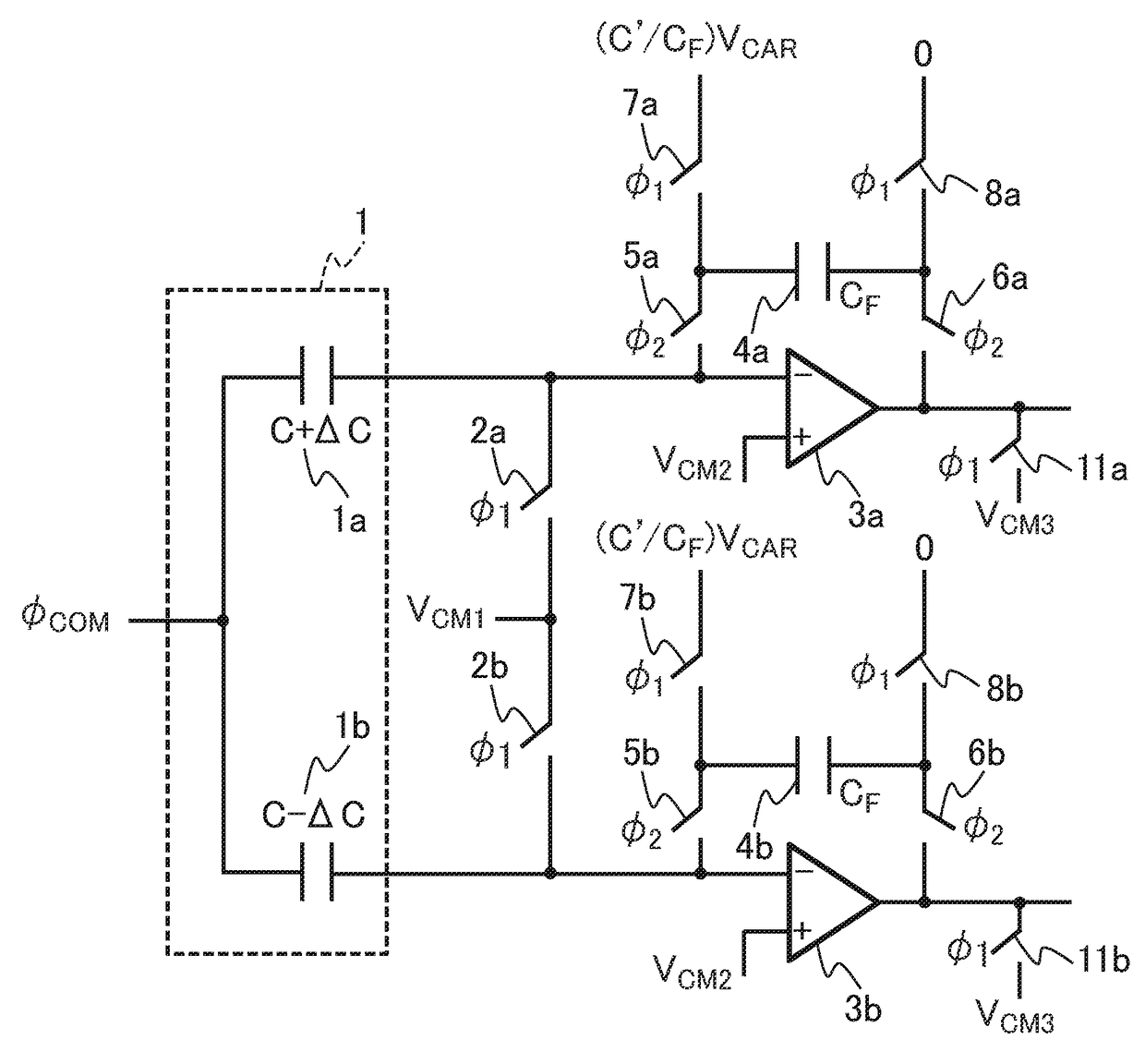
[0060]FIG. 1 shows a first embodiment of the present invention. This is an example in the case of a pseudo-differential CV conversion amplifier. First, configurations will be described.
[0061]A capacitive MEMS 1 includes two detection MEMS capacitive elements 1a and 1b. One of the electrodes of each of the detection MEMS capacitive elements 1a and 1b is a movable electrode that is mechanically movable. The movable electrodes of the detection MEMS capacitive elements 1a and 1b are both connected to a carrier clock φCOM. The other electrodes (fixed electrodes) are connected to the inverting input terminals of operational amplifiers 3a and 3b. The other electrodes are connected to a voltage VCM1 through sampling switches 2a and 2b.
[0062]The turning on and off of the sampling switches 2a and 2b is controlled by a clock signal φ1. Between the inverting input terminal and the output terminal of the operational amplifier 3a, a feedback capacitive element 4a (at a capacitance value CF) is c...
second embodiment
[0078]FIG. 3 is a diagram showing a second embodiment of the present invention. FIG. 4 is an operation timing chart of the second embodiment. The second embodiment is different from the first embodiment in that as illustrated in FIG. 4, the carrier clock φCOM is at a low voltage when the clock signal φ1 is at a high voltage and as illustrated in FIG. 3, forward charging switches 7a and 7b are connected to the ground and forward charging switches 8a and 8b are connected to the charging voltage correspondingly.
[0079]First, in configurations, differences from the first embodiment will be mainly described. Configurations similar to the configurations of the first embodiment are designated the same reference numerals and signs, and the description is omitted. In the second embodiment, the operational amplifier input-side electrode of a feedback capacitive element 4a is connected to the ground (at zero potential) through the forward charging switch 7a, and the operational amplifier output...
third embodiment
[0088]FIG. 5 shows a third embodiment of the present invention. FIG. 6 shows an operation timing chart of the third embodiment. It is an object of the embodiment that a CV conversion amplifier is provided with an amplitude modulation function to convert a low-frequency signal ΔC into a radio-frequency signal for avoiding the influence of 1 / f noise and the direct current offset voltage of the CV conversion amplifier and subsequent analog circuits. In other words, the object is to operate the CV conversion amplifier as a so-called chopper amplifier. This function corresponds to alternately performing the operation of the first embodiment and the operation of the second embodiment.
[0089]In order to achieve this, the difference from the first embodiment is in that first, as illustrated in FIG. 6, the frequency of a carrier clock φCHOP is a half of the frequency of the clock signal φ1 or φ2. Thus, in the relationship between the carrier clock φCHOP and the clock signal φ1, their levels a...
PUM
 Abstract
Description
Claims
Application Information