Opto-Electronic Device With Two-Dimensional Injection Layers

a technology of optoelectronic devices and injection layers, which is applied in the direction of basic electric elements, semiconductor devices, electrical equipment, etc., can solve the problems of reducing the lateral spreading resistance, not allowing significant improvement, and increasing the turn-on voltage of uv led devices

Active Publication Date: 2018-03-01
SENSOR ELECTRONICS TECH
View PDF4 Cites 8 Cited by
  • Summary
  • Abstract
  • Description
  • Claims
  • Application Information

AI Technical Summary

Problems solved by technology

Achieving the necessary p-type doping for efficient operation is a challenge due to high ionization energy of acceptor impurities in these group III nitride materials.
Also, adding the SiO2 / semiconductor interface in this design substantially increases the turn-on voltage of the UV LED device.
In this approach, a high electron concentration in the top group III nitride layer causes carrier tunneling through the tunnel junction and reduces the lateral spreading resistance.
However, this design does not allow for significant improvement in the hole injection into the light generating structure.
This approach results in excessive voltage drop across the additional barrier without any significant increase in the hole injection into the light generating structure.
All of these design approaches for group III nitride based UV LEDs lack the capability to enable high carrier concentration in the light generating structure due to high ionization energy of the doped group III nitride materials.

Method used


Image

  • Opto-Electronic Device With Two-Dimensional Injection Layers
  • Opto-Electronic Device With Two-Dimensional Injection Layers
  • Opto-Electronic Device With Two-Dimensional Injection Layers

Examples


Embodiment Construction

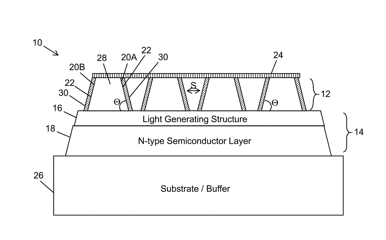
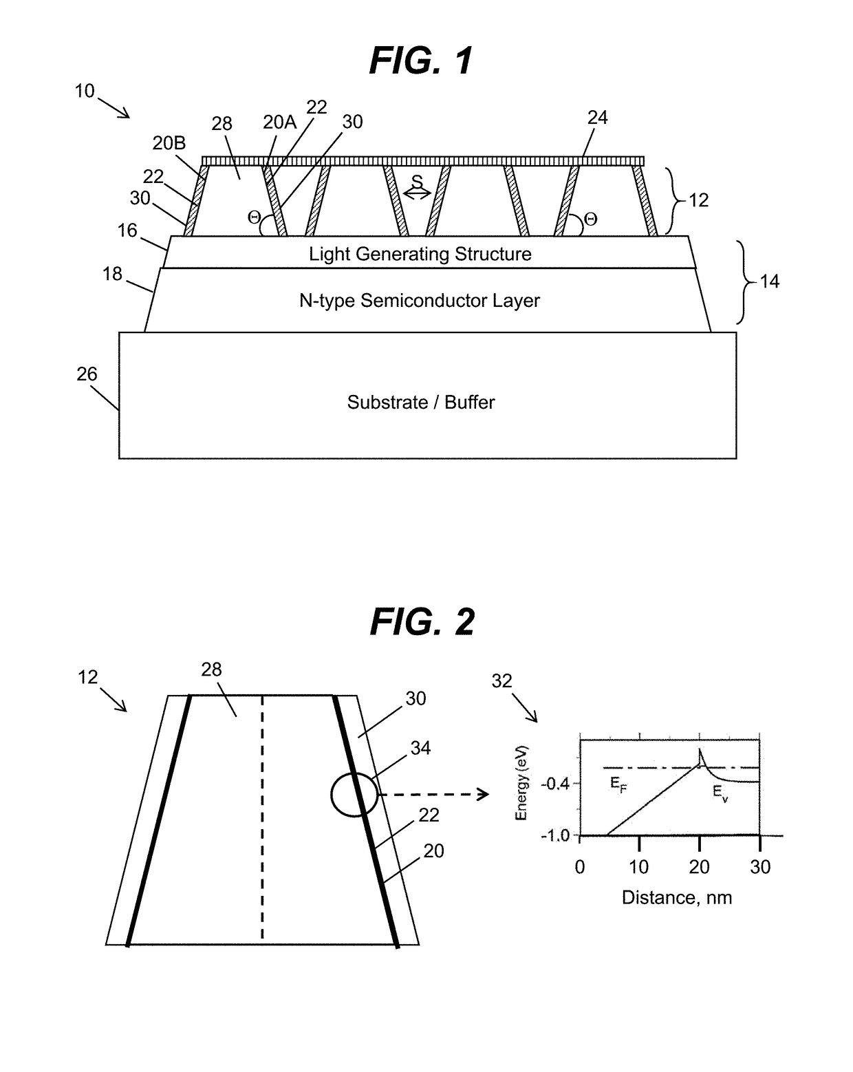
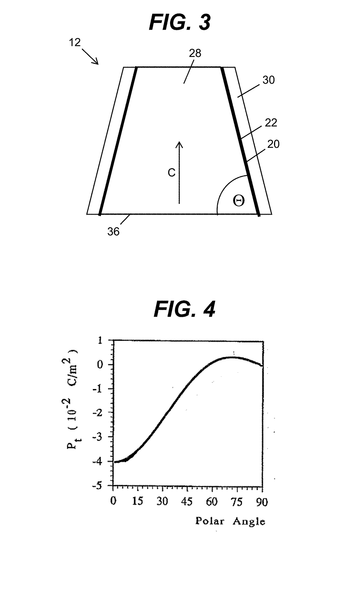
[0049]The various embodiments are directed to improving carrier injection in opto-electronic devices such as UV LEDs. Improved carrier injection is obtained in the various embodiments of the present invention by forming 2DG layers at a heterointerface between two materials with different compositions. In one embodiment, a set of tilted semiconductor heterostructures can be formed over a single or multi-layered semiconductor structure having a light generating structure. Each of the tilted semiconductor heterostructures can include a core region and a set of shell regions that each adjoin a sidewall of the core region. The core region and the set of shell regions can include different compositions of the same material. The heterointerface between the core region and the shell regions leads to the formation of 2DG layers at the interface between the two materials with different compositions.

[0050]As used herein, an opto-electronic device can include any light emitting device or solid ...


PUM


Abstract

An opto-electronic device with two-dimensional injection layers is described. The device can include a semiconductor structure with a semiconductor layer having one of an n-type semiconductor layer or a p-type semiconductor layer, and a light generating structure formed on the semiconductor layer. A set of tilted semiconductor heterostructures is formed over the semiconductor structure. Each tilted semiconductor heterostructure includes a core region, a set of shell regions adjoining a sidewall of the core region, and a pair of two-dimensional carrier accumulation (2DCA) layers. Each 2DCA layer is formed at a heterointerface between one of the sidewalls of the core region and one of the shell regions. The sidewalls of the core region, the shell regions, and the 2DCA layers each having a sloping surface, wherein each 2DCA layer forms an angle with a surface of the semiconductor structure.

Description

REFERENCE TO RELATED APPLICATIONS[0001]The present patent application claims the benefit of U.S. Provisional Application No. 62 / 382,218, filed on 31 Aug. 2016, which is hereby incorporated by reference.TECHNICAL FIELD[0002]The present invention relates generally to opto-electronic devices such as for example, ultraviolet light emitting diodes (UV LEDs), and more particularly, to devices that include tilted semiconductor heterostructures having two-dimensional carrier accumulation (2DCA) layers for improved carrier injection.BACKGROUND ART[0003]A great deal of interest has been focused on UV LEDs and lasers, in particular those that emit light in the blue and deep ultraviolet (UV) wavelengths. These opto-electronic devices may be capable of being incorporated into various applications, including solid-state lighting, biochemical detection, high-density data storage, and the like.[0004]A modern opto-electronic device, such as a UV LED, typically includes three major components: an ele...

Claims


Application Information

Patent Timeline
Patent Type & Authority Applications(United States)
IPC IPC(8): H01L33/24H01L33/06H01L33/08H01L33/14H01L33/32H01L33/40H01L33/44
CPCH01L33/24H01L33/06H01L33/08H01L2933/0091H01L33/32H01L33/405H01L33/44H01L33/14H01L33/20
Inventor SIMIN, GRIGORYSHUR, MICHAELDOBRINSKY, ALEXANDER
Owner SENSOR ELECTRONICS TECH
Why Eureka
Try Eureka