

Textured surfaces for polynucleotide synthesis
- Summary
- Abstract
- Description
- Claims
- Application Information
AI Technical Summary
Benefits of technology
Problems solved by technology
Method used
Image

Examples
example 1
Textured Silicon Arrays
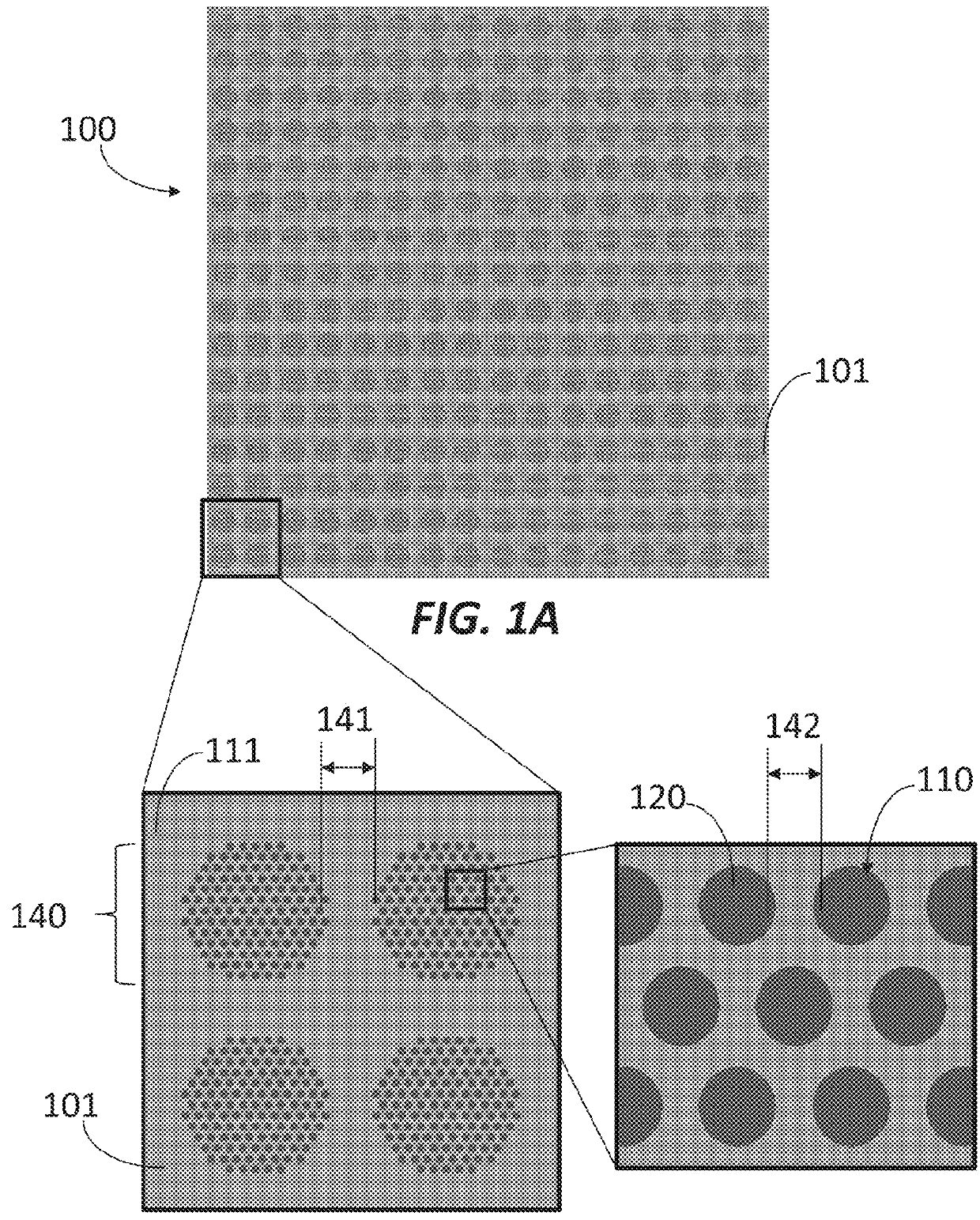
[0246]An array of posts was etched into a silicon dioxide wafer to increase surface area by a factor of 2 to 3. Images of the microfluidic device are shown in FIGS. 18-21. FIGS. 18 and 19 are top view image of the microfluidic device. FIG. 20 is a side-view image at 52 degrees of the microfluidic device at a scale to be able to distinguish the posts of the textured surface. FIG. 21 is a side-view the textured microfluidic device.
[0247]A textured silicon arrays was manufactured having the following features: etched posts measured 746 nm in height, 272 nm wide at the top of the post, and 264 nm wide at the bottom of the post, and a layer of thermal oxide “caps” the posts was s 74 nm thick.
[0248]Additional images of the microfluidic device are shown in FIGS. 22A-22B. FIG. 22A is a side view image of the microfluidic device which highlights the macro geometry of loci. FIG. 22B is a side-view image of the microfluidic device at a scale to be able to distinguish the...
example 2
Design, Manufacturing and Analysis of Arrays Having Textured Loci for Polynucleotide Extension
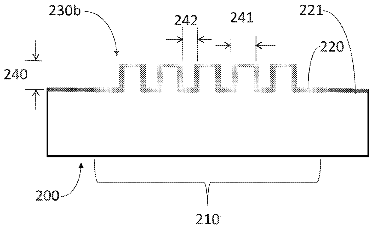
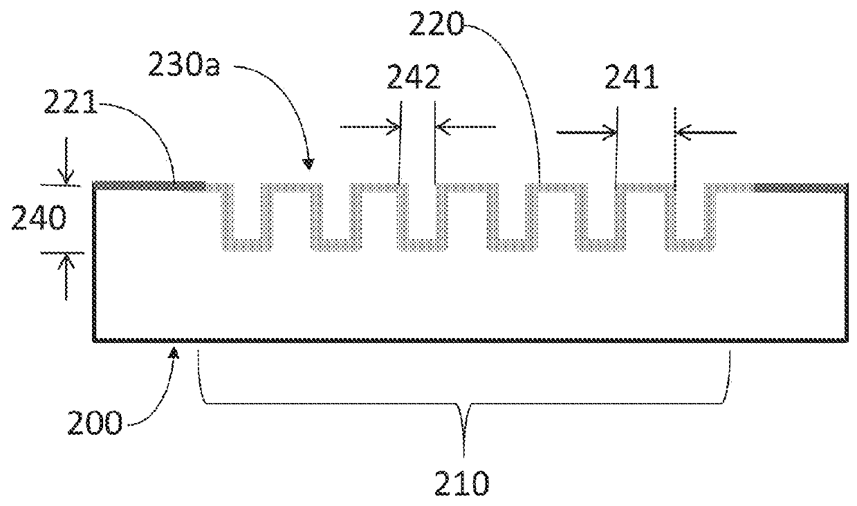
[0253]Array design. Silicon plates were manufactured with the following features designed for etched posts: Array A: oxide “caps” on top of the posts of 122 nm in height; etch depth of post of 301 nm; and post width at the base of 320 nm; and Array B: oxide “caps” on top of the posts of 112 nm in height; etch depth of post of 426 nm; and post width at the base of 316 nm.
[0254]Synthesis on manufactured plates with textured loci. Each of the silicon plates contained an array of clusters, each cluster having discrete locations (“loci”) for nucleotide extension. FIGS. 23A-23B depict low magnification images of a cluster of loci after performing an polynucleotide synthesis reaction. FIG. 23A depicts an image of a cluster of untextured loci. FIG. 23B depicts an image of a cluster of textured loci.
[0255]A silicon plate was manufactured with clusters of loci having three different conditions: untex...
example 3
Patterning of a Wet Deposited Organo-Silicon Containing Molecule
[0266]A silicon dioxide wafer was treated with a single organic layer deposited at different locations on the wafer to create loci with a high surface energy and coupling ability to nucleoside. A surface of 1000 Angstroms of silicon dioxide on top of polished silicon was selected. A controlled surface density of hydroxyl groups was achieved on the surface by a wet process using a 1% solution of N-(3-triethoxysilylpropyl)-4-hydroxybutyramidein ethanol and acetic acid deposited on the surface and treated for 4 hours, followed by placing the wafers on a hot plate at 150 degrees C. for 14 hours.
[0267]A layer of MEGAPOSIT SPR 3612 photoresist was deposited on top of the N-(3-triethoxysilylpropyl)-4-hydroxybutyramide. In this case, the organic layer was an adhesion promoter for the photoresist. The photoresist layer was patterned by exposure to ultraviolet light through a shadow mask. The photoresist pattern was transferred i...
PUM
| Property | Measurement | Unit |
|---|---|---|
| Fraction | aaaaa | aaaaa |
| Fraction | aaaaa | aaaaa |
| Fraction | aaaaa | aaaaa |
Abstract
Description
Claims
Application Information