Supercharge Your Innovation With Domain-Expert AI Agents!

Surface-treated copper foil, manufacturing method therefor, printed circuit board copper-clad laminate, and printed circuit board

a manufacturing method and technology for printed circuit boards, applied in the direction of insulating cables, conductive materials, synthetic resin layered products, etc., can solve the problems of high cost, high cost, and difficult to ensure the high bonding strength between such an extremely thin copper foil and the resin layer, so as to reduce the leakage current, increase peeling strength, and high bonding strength

Active Publication Date: 2018-05-31
MITSUI MINING & SMELTING CO LTD
View PDF11 Cites 1 Cited by
  • Summary
  • Abstract
  • Description
  • Claims
  • Application Information

AI Technical Summary

Benefits of technology

The patent text describes a coating solution for an extremely thin copper foil used in printed wiring boards. This solution involves a silicon-based surface coating layer that contains carbon and oxygen. This coating increases the bonding strength of the copper foil to a resin layer, even if the copper foil is smooth, which can be achieved through vapor deposition, such as sputtering. This solution also provides the copper foil with desirable insulation resistance for achieving a fine pitch in printed wiring boards.

Problems solved by technology

Such an extremely thin copper foil manufactured by an electrolytic deposition technique, however, is likely to have problems, such as pinhole formation due to the excessively small thickness.
The resulting extremely thin copper foil, however, is not expected to have the anchoring effect based on asperities on the copper foil surface because of its extremely smooth surface (e.g., arithmetic mean roughness Ra: 200 nm or less).
Thus, it has been difficult to ensure the high bonding strength between such an extremely thin copper foil and the resin layer.

Method used


Image

  • Surface-treated copper foil, manufacturing method therefor, printed circuit board copper-clad laminate, and printed circuit board
  • Surface-treated copper foil, manufacturing method therefor, printed circuit board copper-clad laminate, and printed circuit board
  • Surface-treated copper foil, manufacturing method therefor, printed circuit board copper-clad laminate, and printed circuit board

Examples


examples

[0044]The present invention will be described in further detail by the following examples.

examples 1 to 8

[0045](1) Preparation of a Copper Foil Provided with a Carrier

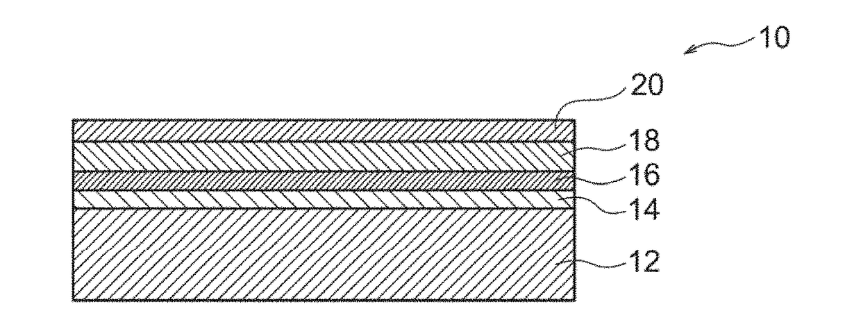
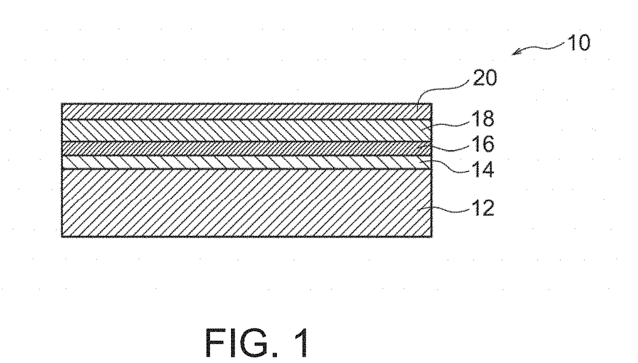
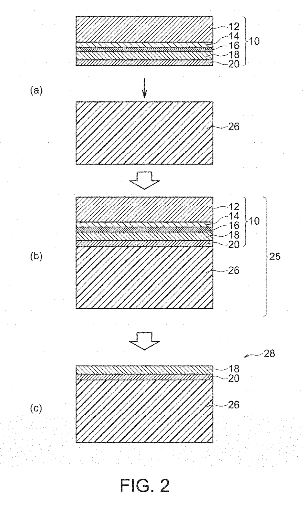
[0046]As shown in FIG. 1, a refractory metal layer 14, a release layer 16, an extremely thin copper foil layer 18, and a silicon-based surface coating layer 20 were formed in this order on a carrier 12 of electrodeposited copper foil to prepare a copper foil 10 provided with a carrier. The silicon-based surface coating layer 20 was formed according to the various conditions shown in Table 1. The detailed procedures are as follows.

[0047](1a) Preparation of carrier

[0048]An electrodeposited copper foil with a thickness of 18 μm and a glossy surface having an arithmetic mean roughness Ra of 60 to 70 nm (Mitsui Mining & Smelting Co.) was provided as a carrier foil 12. The carrier was cleaned by pickling. The pickling was performed by immersing the carrier in a diluted sulfuric acid solution having a sulfuric acid concentration of 150 g / I at a temperature of 30° C. for 30 sec to remove the surface oxide layer, followed by rinsi...


PUM

PropertyMeasurementUnit
Thicknessaaaaaaaaaa
Thicknessaaaaaaaaaa
Percent by atomaaaaaaaaaa

Abstract

There is provided a copper foil having a surface coating layer that can achieve a high bonding strength to a resin layer even if the copper foil has an extremely smooth surface such as one formed by vapor deposition, for example, sputtering and also has a desirable insulation resistance suitable for achieving a fine pitch in a printed wiring board. A surface-treated copper foil according to the present invention includes a copper foil and a silicon-based surface coating layer provided on at least one surface of the copper foil, the silicon-based surface coating layer being mainly composed of silicon (Si). The silicon-based surface coating layer has a carbon content of 1.0 to 35.0 atomic % and an oxygen content of 12.0 to 40.0 atomic % relative to a total content in 100 atomic % of carbon (C), oxygen (O) and silicon (Si) elements as measured by X-ray photoelectron spectroscopy (XPS).

Description

TECHNICAL FIELD[0001]The present invention relates to a surface-treated copper foil, a method for manufacturing the surface-treated copper foil, a copper-clad laminate for a printed wiring board, and a printed wiring board.BACKGROUND ART[0002]In recent years, downsizing and sophistication of electronic devices, such as portable electronic devices, demand printed wiring boards having further miniaturized (fine-pitched) wiring patterns. To meet such a requirement, a copper foil for manufacturing a printed wiring board is desired to have a smaller thickness and a lower surface roughness than current ones.[0003]The copper foil for manufacturing a printed wiring board is used in lamination to an insulating resin substrate. It is important to ensure bonding strength between the copper foil and the insulating resin substrate because low bonding strength may cause traces to separate during manufacturing the printed wiring board, resulting in a low product yield. In this regard, usual copper...

Claims


Application Information

Patent Timeline
IPC IPC(8): H01B1/02H01B3/46H01B7/02H05K1/03B32B15/04
CPCH01B1/026H01B3/46H01B7/02H05K1/036H05K1/0306B32B15/04C23C14/06H05K3/025H05K3/388H05K2201/0179H05K2201/029B32B5/022B32B5/024B32B27/08B32B29/005B32B2250/03B32B2250/04B32B27/28B32B27/285B32B27/42B32B27/20B32B27/38B32B2255/205B32B2255/20B32B2255/26B32B2255/28B32B2255/10B32B2260/021B32B2260/046B32B2260/028B32B2262/101B32B2264/101B32B2307/406B32B2307/5825B32B2307/732B32B2307/538B32B2457/08B32B17/061B32B15/20B32B7/06C23C14/165C23C14/3414C23C14/0036H05K1/03H05K3/38
Inventor MATSUURA, YOSHINORI
Owner MITSUI MINING & SMELTING CO LTD
Features
  • R&D
  • Intellectual Property
  • Life Sciences
  • Materials
  • Tech Scout
  • Unparalleled Data Quality
  • Higher Quality Content
  • 60% Fewer Hallucinations
Learn More