Light-Emitting Element, Light-Emitting Device, Electronic Device, Display Device, and Lighting Device

Inactive Publication Date: 2018-05-31
SEMICON ENERGY LAB CO LTD
View PDF0 Cites 5 Cited by
  • Summary
  • Abstract
  • Description
  • Claims
  • Application Information

AI Technical Summary

Benefits of technology

[0010]An object of one embodiment of the present invention is to prov

Problems solved by technology

The BT.2020 standard can express almost all object colors; however, it is difficult under the present conditions to achieve it simply by using a broad emission spectrum of an organic compound as it is.
Thus, the color purity which enables the satisfaction of the a

Method used


Image

  • Light-Emitting Element, Light-Emitting Device, Electronic Device, Display Device, and Lighting Device
  • Light-Emitting Element, Light-Emitting Device, Electronic Device, Display Device, and Lighting Device
  • Light-Emitting Element, Light-Emitting Device, Electronic Device, Display Device, and Lighting Device

Examples


embodiment 1

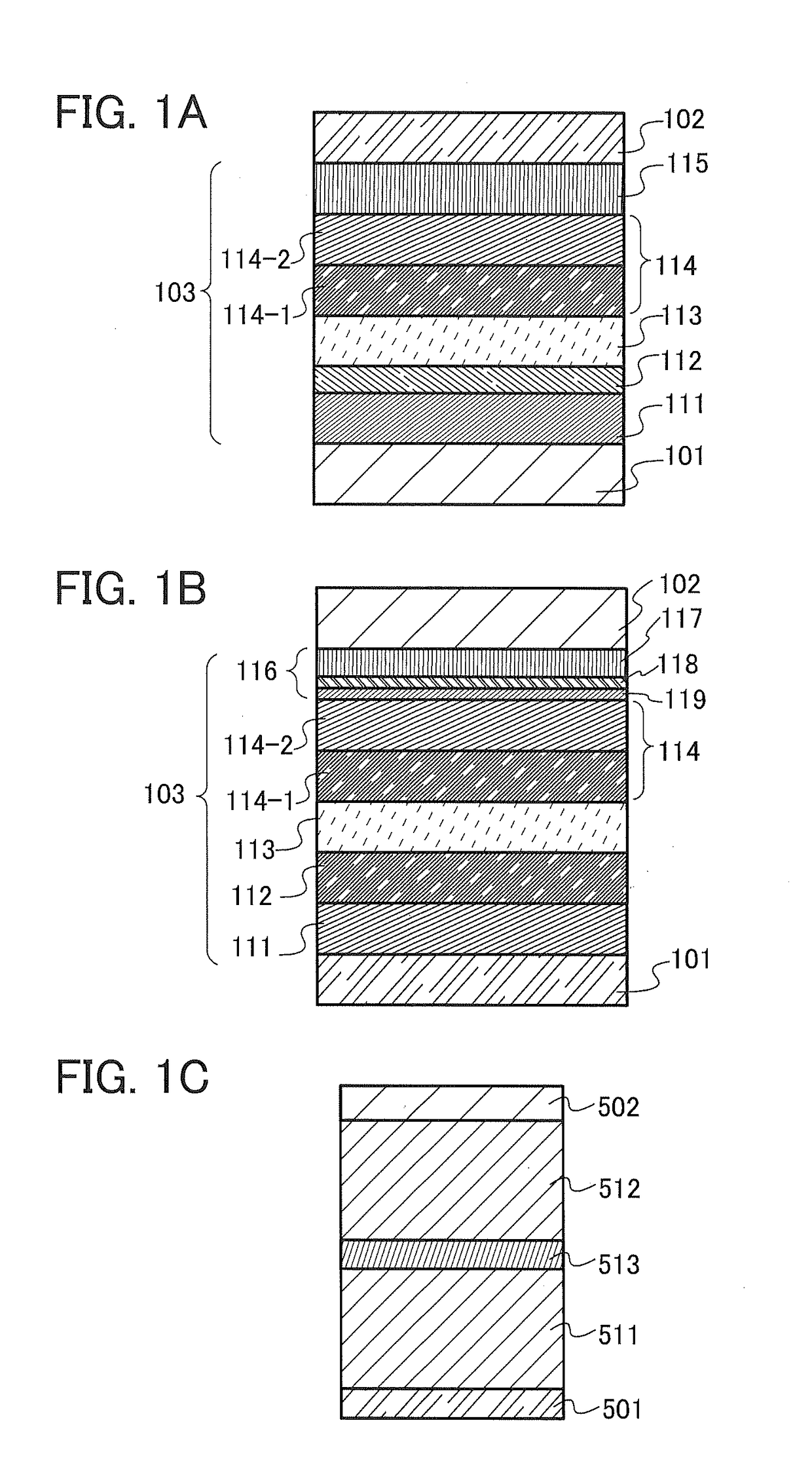
[0062]A metal-halide perovskite material is a composite material of an organic material and an inorganic material or a material formed of only an inorganic material, and has some interesting properties such as light emission by excitons or high carrier mobility. The metal-halide perovskite material has a superstructure in which inorganic layers (also referred to as perovskite layers) and organic layers are alternately stacked, which forms a quantum well structure. Therefore, the metal-halide perovskite material exhibits particularly high exciton binding energy, so that excitons can exist stably. Furthermore, the metal-halide perovskite material has a narrow half width and exhibits light emission by exciton with a small Stokes shift; thus, usage in a light-emitting element is expected. Moreover, a quantum dot of the metal-halide perovskite material is also known as a substance that exhibits favorable color-purity light emission with an extremely narrow half width.

[0063]In addition, b...

embodiment 2

[0150]In this embodiment, a light-emitting device including a light-emitting element described in Embodiment 1 will be described.

[0151]A light-emitting device of one embodiment of the present invention will be described with reference to FIGS. 4A and 4B. Note that FIG. 4A is a top view of the light-emitting device and FIG. 4B is a cross-sectional view taken along the lines A-B and C-D in FIG. 4A. The light-emitting device includes a driver circuit portion (source line driver circuit) 601, a pixel portion 602, and a driver circuit portion (gate line driver circuit) 603 which are illustrated with dotted lines. Furthermore, reference numeral 604 denotes a sealing substrate and reference numeral 605 denotes a sealant. A portion surrounded by the sealant 605 is a space 607.

[0152]Note that a lead wiring 608 is a wiring for transmitting signals to be input to the source line driver circuit 601 and the gate line driver circuit 603 and for receiving a video signal, a clock signal, a start si...

example 1

[0277]In this example, fabrication methods and characteristics of light-emitting elements of one embodiment of the present invention and a comparative light-emitting element will be described in detail.

(Fabrication Method of Light-Emitting Element 1)

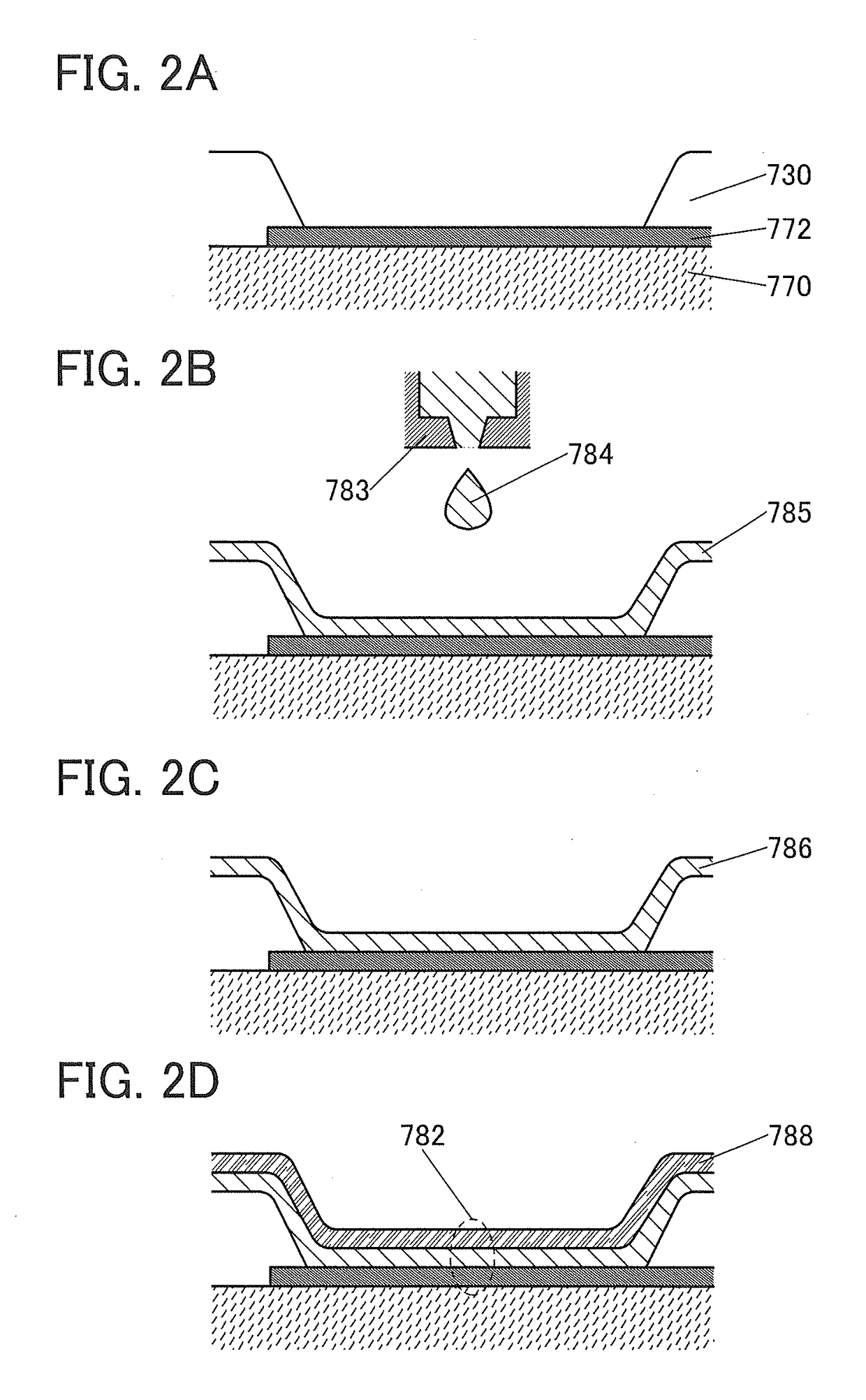
[0278]First, a film of indium tin oxide including silicon oxide (ITSO) was formed over a glass substrate by a sputtering method, so that the anode 101 was formed. The film thickness was 70 nm and the electrode area was 2 mm×2 mm.

[0279]Next, pretreatment for forming the light-emitting element over the substrate was performed, in which a surface of the substrate was washed with water and baked at 200° C. for 1 hour, and then UV ozone treatment was performed for 370 seconds.

[0280]Then, the substrate was fixed to a substrate holder of a spin coater so that a surface on the anode 101 side faced upward, and an aqueous solution of poly(3,4-ethylenedioxythiophene) / poly(styrenesulfonic acid) (PEDOT / PSS) purchased from H.C. Starck (Product No. CRE...


PUM

PropertyMeasurementUnit
Lengthaaaaaaaaaa
Nanoscale particle sizeaaaaaaaaaa
Efficiencyaaaaaaaaaa

Abstract

A novel light-emitting element is provided. A light-emitting element with high emission efficiency is provided. A light-emitting element with high color purity is provided. The light-emitting element includes an anode, a cathode, and a layer including the light-emitting substance between the anode and the cathode. The layer including the light-emitting substance includes a light-emitting layer, a first electron-transport layer, and a second electron-transport layer. The light-emitting layer and the first electron-transport layer are in contact with each other. The first electron-transport layer and the second electron-transport layer are in contact with each other. The first electron-transport layer and the second electron-transport layer are positioned between the light-emitting layer and the cathode. The light-emitting layer includes a metal-halide perovskite material represented by General Formula (SA)MX3, General Formula (LA)2(SA)n-1MnX3n+1, or General Formula (PA)(SA)n-1MnX3n+1. The first electron-transport layer includes a first electron-transport material, and the second electron-transport layer includes a second electron-transport material.

Description

BACKGROUND OF THE INVENTION1. Field of the Invention[0001]One embodiment of the present invention relates to a light-emitting element, a display module, a lighting module, a display device, a light-emitting device, an electronic device, and a lighting device. Note that one embodiment of the present invention is not limited to the above technical field. The technical field of one embodiment of the invention disclosed in this specification and the like relates to an object, a method, or a manufacturing method. Furthermore, one embodiment of the present invention relates to a process, a machine, manufacture, or a composition of matter. Specifically, examples of the technical field of one embodiment of the present invention disclosed in this specification include a semiconductor device, a display device, a liquid crystal display device, a light-emitting device, a lighting device, a power storage device, a storage device, an imaging device, a method for driving any of them, and a method ...

Claims


Application Information

Patent Timeline
IPC IPC(8): H01L51/00H01L51/50C09K11/06
CPCH01L51/0077H01L51/508H01L51/0037H01L51/0035C09K11/06H01L51/0072H01L51/0058H01L51/5092H01L51/5012H01L51/0005H01L27/3244H01L27/3213H01L27/3281H01L51/56C09K2211/18H10K85/00H10K50/16H10K50/11H10K59/38H10K59/17H10K71/135H10K59/12H10K85/30H10K50/166H10K85/50H10K85/655H10K85/6572H10K50/165H10K85/111H10K85/626H10K85/1135H10K50/171H10K59/351H10K71/00
Inventor HIROSE, TOMOYASEO, SATOSHITSUTSUI, TETSUO
Owner SEMICON ENERGY LAB CO LTD
Why Eureka
Try Eureka