Methods of making wiring substrate for stackable semiconductor assembly and making stackable semiconductor assembly

a stackable semiconductor and wiring substrate technology, applied in semiconductor devices, semiconductor/solid-state device details, electrical devices, etc., can solve problems such as sudden device failure and i/o disconnection, unreliable practical use of stacking structures, and solder cracking, so as to improve routing flexibility of wiring substrates

Active Publication Date: 2018-06-07
BRIDGE SEMICON
View PDF14 Cites 15 Cited by
  • Summary
  • Abstract
  • Description
  • Claims
  • Application Information

AI Technical Summary

Benefits of technology

[0007]An objective of the present invention is to provide a method of making a wiring substrate having a cavity by etching of a sacrificial metal slug at a designated location. As this sacrificial metal slug is mechanically supported and physically surrounded by a resin compound, once a selected portion of metal is removed, a cavity with well-defined size and depth can be formed and surrounded by the resin compound, thereby allowing a device to be disposed in the cavity without contributing much thickness to the final assembly.
[0008]Another objective of the present invention is to provide a method of making a wiring substrate having vertical stacking channel by providing a plurality of metal leads surrounding a cavity. As a result, a device disposed in the cavity can be stacked with another device through the metal leads without the need for other external interconnection.
[0009]Yet another objective of the present invention is to provide a method of making a wiring substrate with all the elements bonded together by a resin compound, thereby allowing a stable mechanical structure that can endure thermal cycling without suffering solder cracking, warping or dislocation.
[0010]Yet another objective of the present invention is to provide a method of making a wiring substrate optionally having a routing circuitry so that the electrical signal can be re-distributed from the peripheral leads to the designated location and the electrical characteristics of the resulting semiconductor assembly can be greatly improved.
[0013]The methods of making a wiring substrate and making the related 3D stackable semiconductor assembly using the wiring substrate according to the present invention have numerous advantages. For instance, providing the metal leads around the cavity is particularly advantageous as the semiconductor device can be disposed in the cavity and the metal leads can be electrically connected to the semiconductor device by the bonding wires and offer horizontal routing and vertical connecting channels between two opposites side of the wiring substrate. As the semiconductor device is disposed in the cavity, no extra grinding or lapping is needed for the semiconductor device in order to achieve ultra-thin vertically stacked semiconductor assembly feature. Binding the resin compound to the metal leads can provide a integral platform for high resolution circuitries disposed thereon. Depositing the re-distribution layer on the resin compound can enhance routing flexibility of the wiring substrate and allow fine pitch assemblies such as flip chip and surface mount component to be assembled thereon and interconnected to the metal leads by the re-distribution layer.

Problems solved by technology

As the substrate is a stacked structure, warpage or thermal expansion coefficient (CTE) mismatches between these two parts will result in dislocation or solder cracking, making this kind of stacking structure unreliable for practical usage.
Again, solder deforming and cracking in the encapsulation, or delamination between the encapsulant and the substrate after thermal cycling may lead to abrupt device failure and I / O disconnection.

Method used


Image

  • Methods of making wiring substrate for stackable semiconductor assembly and making stackable semiconductor assembly
  • Methods of making wiring substrate for stackable semiconductor assembly and making stackable semiconductor assembly
  • Methods of making wiring substrate for stackable semiconductor assembly and making stackable semiconductor assembly

Examples


embodiment 1

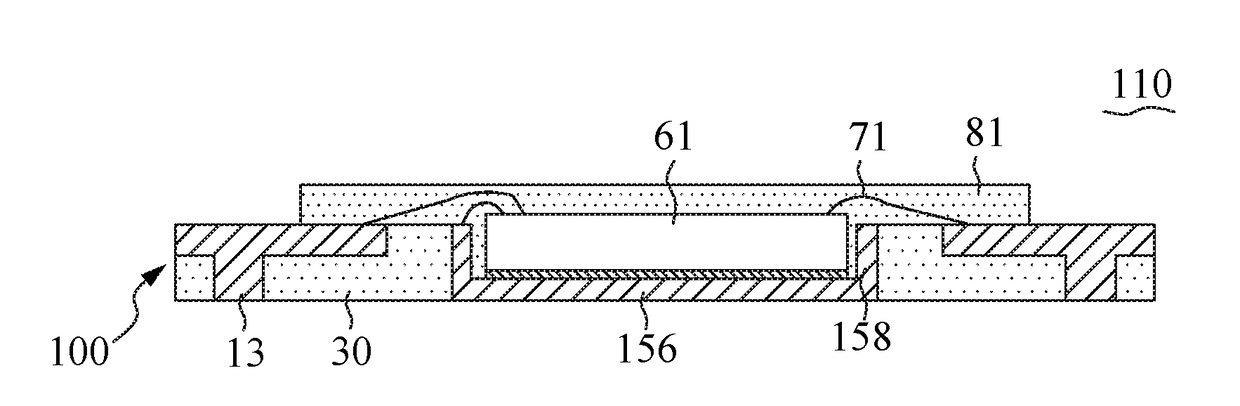
[0054]FIGS. 1-16 are schematic views showing a method of making a semiconductor assembly that includes a plurality of metal leads, a metal paddle, a metal film, a resin compound, a semiconductor device, a plurality of bonding wires and a molding compound in accordance with the first embodiment of the present invention.

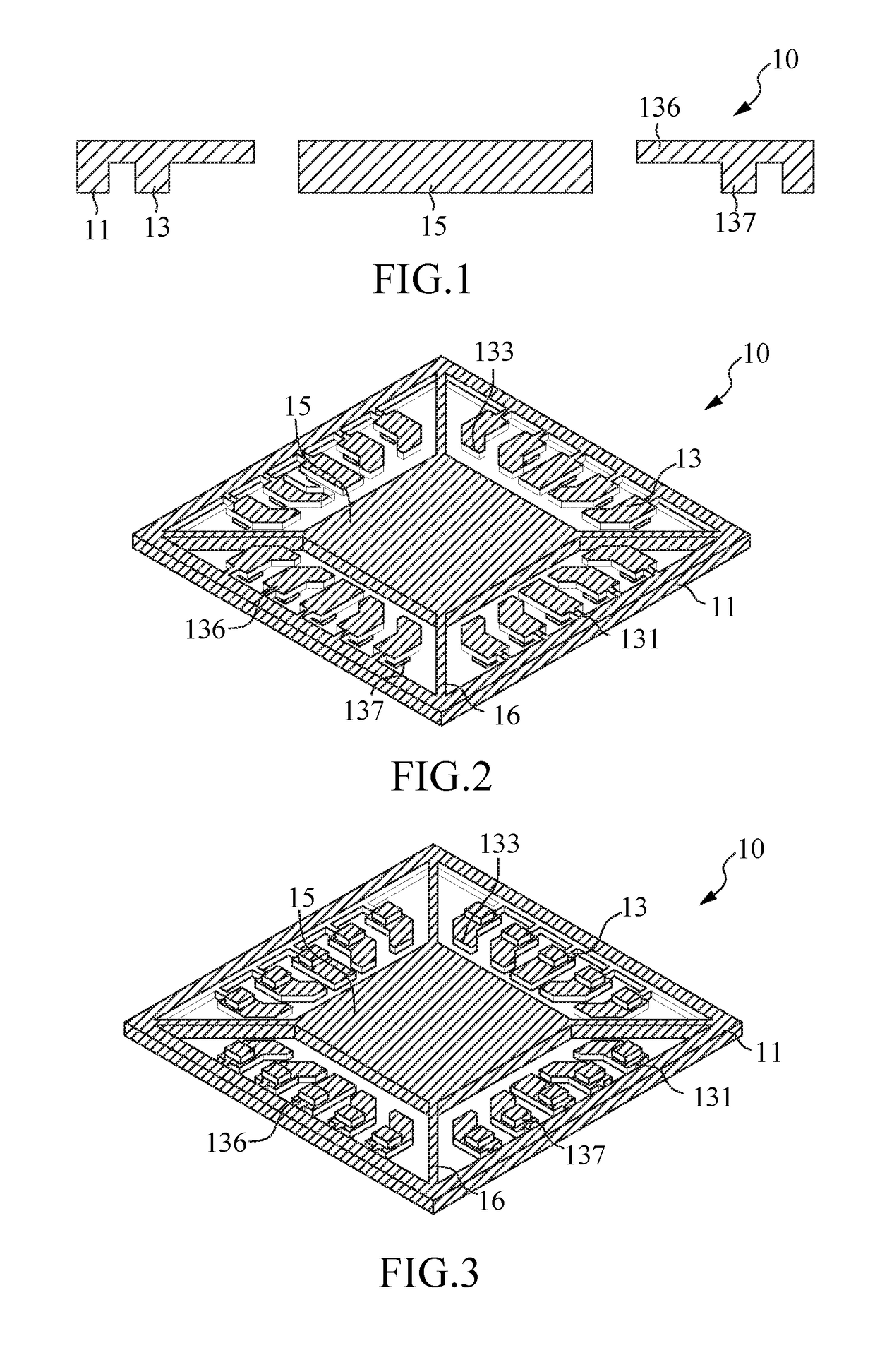
[0055]FIGS. 1, 2 and 3 are cross-sectional, top and bottom perspective views, respectively, of a textured metal sheet 10. The textured metal sheet 10 typically is made of copper alloys, steel or alloy 42, and can be formed by a wet etching or stamping / punching process from a rolled metal strip having a thickness in a range from about 0.15 mm to about 1.0 mm. The etching process may be a one-sided or two-sided etching to etch through the metal strip and thereby transfer the metal strip into a desired overall pattern of the textured metal sheet 10 that includes a metal frame 11, a plurality of metal leads 13, a metal slug 15 and a plurality of tie bars 16. The metal lead...

embodiment 2

[0077]FIGS. 38-45 are schematic views showing a method of making a wiring substrate having a bottom build-up circuitry in accordance with the second embodiment of the present invention.

[0078]For purposes of brevity, any description in Embodiment 1 is incorporated herein insofar as the same is applicable, and the same description need not be repeated.

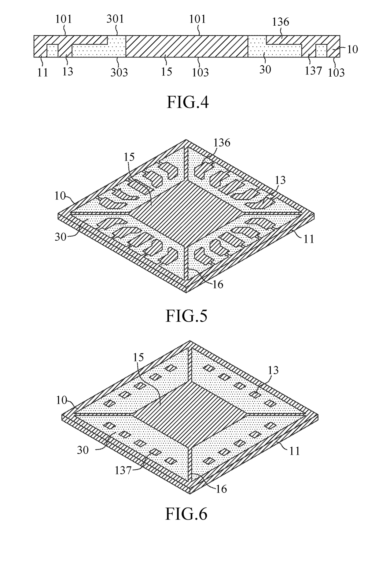
[0079]FIGS. 38 and 39 are cross-sectional and bottom perspective views, respectively, of the structure of FIG. 4 after removal of the metal frame 11. Removal of the metal frame 11 can be done by various methods including chemical etching or mechanical trimming / cutting. By separating the metal frame 11, the connection between the metal leads 13 is broken. As a result, the textured metal sheet 10 includes the metal leads 13, the metal slug 15 and the tie bars 16.

[0080]FIGS. 40 and 41 are cross-sectional and bottom perspective views, respectively, of the structure with a dielectric layer 531 formed on the textured metal sheet 10 and the res...

embodiment 3

[0087]FIGS. 50-61 are schematic views showing a method of making a semiconductor assembly having a semiconductor device attached on a resin paddle in accordance with the third embodiment of the present invention.

[0088]For purposes of brevity, any description in Embodiments above is incorporated herein insofar as the same is applicable, and the same description need not be repeated.

[0089]FIG. 50 is a cross-sectional view of a textured metal sheet 10. The textured metal sheet 10 is similar to that illustrated in FIGS. 1-3, except that it includes no tie bars and the metal slug 15 is thinner than the metal frame 11 and the metal leads 13.

[0090]FIGS. 51 and 52 are cross-sectional and bottom perspective views, respectively, of the structure provided with a resin compound 30 and a resin paddle 40. The resin compound 30 covers the lower surfaces of the horizontally elongated portions 136 as well as sidewalls of the vertically projected portions 137 and sidewalls of the metal slug 15. The r...


PUM


Abstract

The wiring substrate includes a cavity and a plurality of metal leads disposed around the cavity. The metal leads are bonded with a resin compound and provide horizontal and vertical routing for a semiconductor device to be disposed in the cavity. The resin compound fills in spaces between the metal leads and surrounds the cavity and provides a dielectric platform for a re-distribution layer or a build-up circuitry optionally deposited thereon.

Description

CROSS REFERENCE TO RELATED APPLICATIONS[0001]This application is a continuation-in-part of U.S. application Ser. No. 15 / 642,253 filed Jul. 5, 2017, a continuation-in-part of U.S. application Ser. No. 15 / 642,256 filed Jul. 5, 2017, a continuation-in-part of U.S. application Ser. No. 15 / 787,366 filed Oct. 18, 2017 and a continuation-in-part of U.S. application Ser. No. 15 / 863,998 filed Jan. 8, 2018.[0002]The U.S. application Ser. No. 15 / 642,253 is a continuation-in-part of U.S. application Ser. No. 14 / 621,332 filed Feb. 12, 2015 and a continuation-in-part of U.S. application Ser. No. 14 / 846,987 filed Sep. 7, 2015. The U.S. application Ser. No. 15 / 787,366 is a continuation-in-part of U.S. application Ser. No. 15 / 247,443 filed Aug. 25, 2016. The U.S. application Ser. No. 15 / 863,998 is a continuation-in-part of U.S. application Ser. No. 14 / 621,332 filed Feb. 12, 2015, a continuation-in-part of U.S. application Ser. No. 14 / 846,987 filed Sep. 7, 2015, a continuation-in-part of U.S. applica...

Claims


Application Information

Patent Timeline
Patent Type & Authority Applications(United States)
IPC IPC(8): H01L23/498H01L25/10H01L21/48H01L23/00H01L23/31
CPCH01L23/49861H01L25/105H01L21/4803H01L21/4828H01L24/73H01L24/48H01L21/4846H01L23/3185H01L2224/73265H01L2224/48257H01L2224/48247H01L2924/1715H01L2924/15153H01L2924/182H01L2225/1041H01L2225/1058H01L23/13H01L23/49548H01L23/3121H01L23/49838H01L2224/32225H01L2224/32245H01L2924/19105H01L2924/00014H01L2924/00H01L2224/45099H01L2924/00012
Inventor LIN, CHARLES W. C.WANG, CHIA-CHUNG
Owner BRIDGE SEMICON
Why Eureka
Try Eureka