Electronically Abrupt Borophene/Organic Lateral Heterostructures and Preparation Thereof

a technology of organic lateral heterostructure and borophene, which is applied in the direction of non-metal conductors, sustainable manufacturing/processing, and final product manufacturing, etc., can solve the problems of boron showing significantly more complex and diverse bulk structure, difficult methods for experimentally realizing atomically clean and abrupt lateral heterojunctions, and ill-defined interfacial regions

Active Publication Date: 2018-08-09
NORTHWESTERN UNIV
View PDF2 Cites 6 Cited by
  • Summary
  • Abstract
  • Description
  • Claims
  • Application Information

AI Technical Summary

Benefits of technology

[0007]It can be another object of the present invention to provide such heterostructures without alloying or boron compound formation.

Problems solved by technology

Unlike the naturally layered structures of bulk graphite and black phosphorus, boron exhibits significantly more complex and diverse bulk structures due to the rich bonding configurations among boron atoms.
It should be noted, however, that methods for experimentally realizing atomically clean and abrupt lateral heterojunctions remain challenging for many 2D material systems.
For example, the growth front of the first 2D material can be easily contaminated, which can disrupt the subsequent growth of the second 2D material and / or lead to ill-defined interfacial regions.

Method used


Image

  • Electronically Abrupt Borophene/Organic Lateral Heterostructures and Preparation Thereof
  • Electronically Abrupt Borophene/Organic Lateral Heterostructures and Preparation Thereof
  • Electronically Abrupt Borophene/Organic Lateral Heterostructures and Preparation Thereof

Examples


example 1

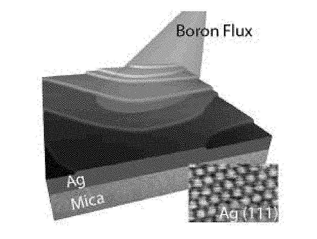
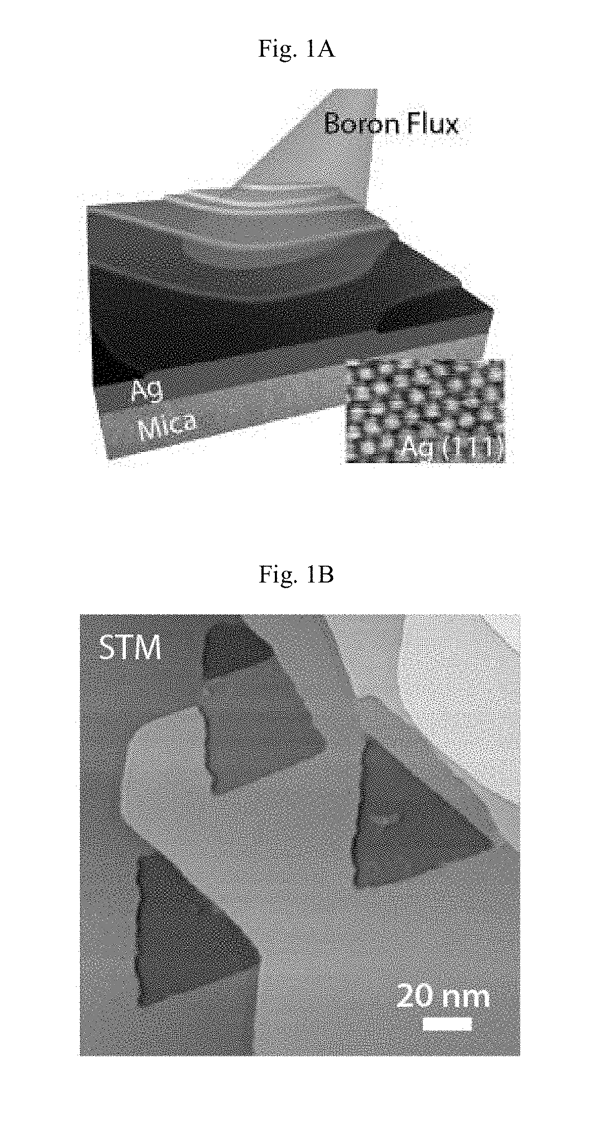
[0053]Growth of borophene / PTCDA lateral heterostructures. All growth is performed in a UHV preparation chamber (pressure −9 Torr) that is directly connected to a loadlock, STM, and XPS system. Ag(111) thin films (˜300 nm thick) on mica substrates (Princeton Scientific Corp.) are cleaned by repeated Ar ion sputtering at 3.3×10⁻⁶ Torr (30 min) followed by annealing at 550° C. (30 min). The deposition of boron is achieved by electron-beam evaporation (SPECS EBE-1) of a pure boron rod (ESPI metals, 99.9999% purity) onto the cleaned Ag(111) substrates held at 480° C. The deposition flux is measured by the flux electrodes of the evaporator and is maintained at 20 to 28 nA with a filament current of ˜5.8 A and accelerating voltage of 1.3 to 1.6 kV. The typical deposition time is 20-30 min to achieve submonolayer coverage of borophene. The electron-beam evaporator is housed in a separately pumped chamber with a base pressure of 8×10⁻¹¹ Torr, and the boron rod is degassed for >6 hr preceding...

example 2

[0054]Scanning Tunneling Microscopy and Spectroscopy.

[0055]A home-built UHV STM (˜10−10 Torr) is used for STM / STS characterization at room temperature with a Lyding-design microscope. (See, E. T. Foley, N. L. Yoder, N. P. Guisinger, M. C. Hersam, Cryogenic variable temperature ultrahigh vacuum scanning tunneling microscope for single molecule studies on silicon surfaces, Rev. Sci. Instrum. 75, 5280-5287 (2004). However, conventional, commercially-available instrumentation can be used with comparable effect.) The bias voltage is applied to the sample with respect to the electrochemically etched PtIr tip (Keysight). The piezo-scanner is calibrated against the Ag(111) lattice (x y) and atomic step height (z). Nanonis (SPECS) control electronics are used for data collection. STS measurements are carried out with a lock-in amplifier (SRS model SR850) with 30 mVRMS amplitude and ˜8.5 kHz modulation frequency. Stable and reproducible spectroscopy was achieved following tip conditioning tha...

example 3

[0056]X-Ray Photoelectron Spectroscopy.

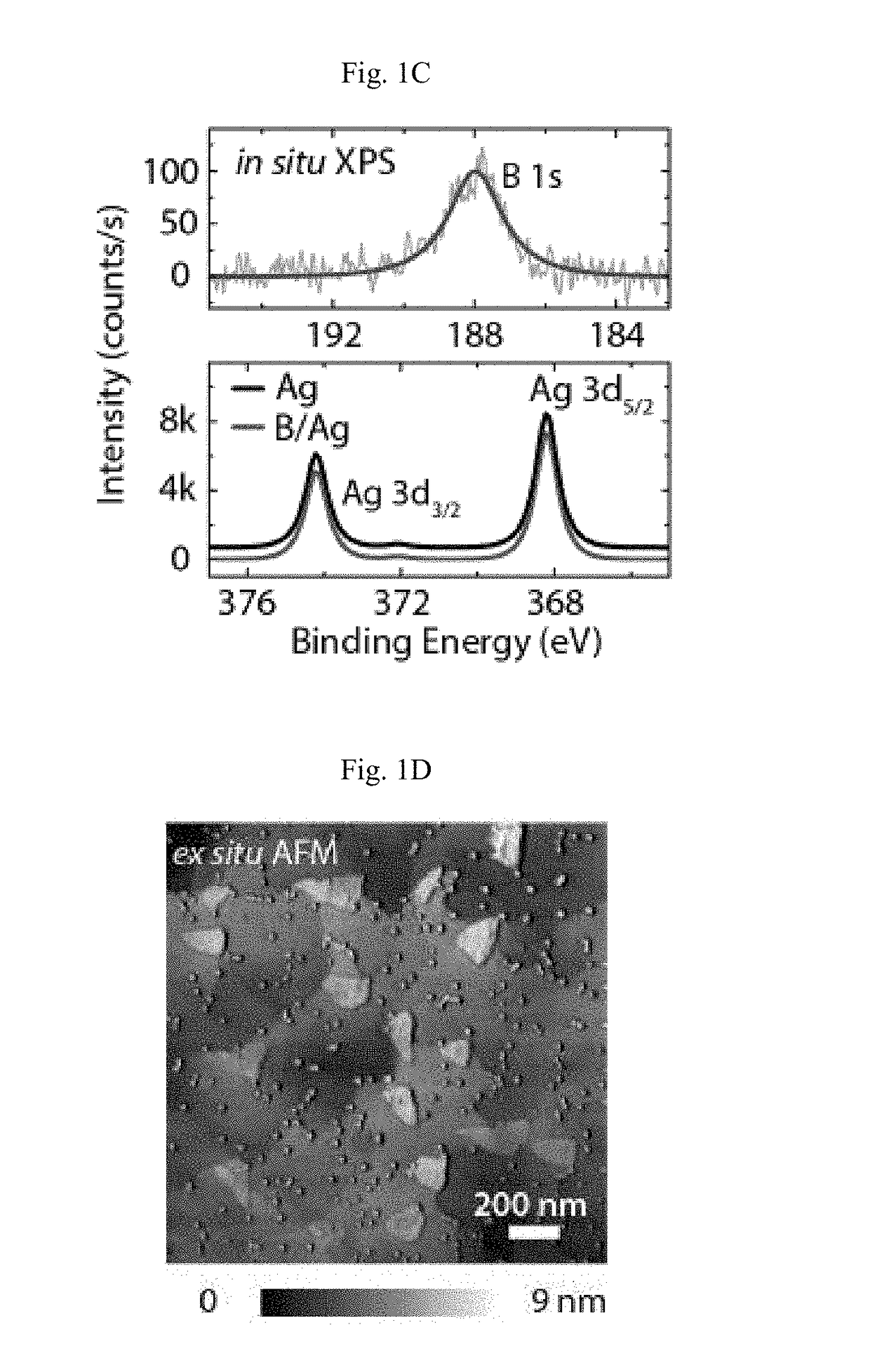
[0057]In situ XPS spectra are taken with an Omicron DAR 400 M X-ray source (Al Kα), XM 500 X-ray monochromator, and EA 125 energy analyzer in a UHV chamber (3×10⁻¹⁰ Torr) that is integrated with the STM system and preparation chamber. The XPS energy resolution is 0.6 eV using a pass-energy of 20 eV for core-level spectra. Modified Shirley backgrounds have been subtracted using Avantage (Thermo Scientific) software. Given the trace amount of adventitious carbon for the clean Ag(111) surface (FIG. 16), all peaks are fitted after calibrating the spectra to the Ag 3d5 / 2 core-level peak (368.2 eV). This calibration is validated by 5 / 2 peaks (FIG. 3) for clean Ag(111), borophene / Ag(111), and PTCDA / borophene / Ag(111) in consecutive runs.


PUM

PropertyMeasurementUnit
binding energyaaaaaaaaaa
thickaaaaaaaaaa

Abstract

Articles comprising a boron allotrope and an organic compound having a lateral interface one with the other, together with method(s) of preparation of such articles.

Description

[0001]This application claims priority to and the benefit of application Ser. No. 62 / 499,938 filed on Feb. 8, 2017, the entirety of which is incorporated herein by reference.[0002]This invention was made with government support under N00014-14-1-0669 awarded by the Office of Naval Research and DMR-1121262 awarded by the National Science Foundation. The government has certain rights in the invention.BACKGROUND OF THE INVENTION[0003]The rapid ascent of graphene has driven extensive interest in additional atomically thin elemental two-dimensional (2D) materials including phosphorene, stanene, and most recently, borophene. (See, A. J. Mannix, X.-F. Zhou, B. Kiraly, J. D. Wood, D. Alducin, B. D. Myers, X. Liu, B. L. Fisher, U. Santiago, J. R. Guest, M. J. Yacaman, A. Ponce, A. R. Oganov, M. C. Hersam, N. P. Guisinger, Synthesis of borophenes: Anisotropic, two-dimensional boron polymorphs, Science 350, 1513-1516 (2015)). Unlike the naturally layered structures of bulk graphite and black p...

Claims


Application Information

Patent Timeline
Patent Type & Authority Applications(United States)
IPC IPC(8): C01B35/04C23C16/04C23C16/22H01L51/00
CPCC01B35/04C23C16/04C23C16/22H01L51/0011H01L51/0053H01L51/0096C01P2002/20C01P2002/60C01P2004/90C01P2006/40C01P2006/90H01L2251/301C23C14/04C23C14/12C23C14/24Y02E10/549Y02P70/50H10K85/621H10K85/322B05D5/12H01B1/06H10K71/166H10K77/10H10K2102/00
Inventor HERSAM, MARK C.LIU, XIAOLONG
Owner NORTHWESTERN UNIV
Why Eureka
Try Eureka