Four junction solar cell and solar cell assemblies for space applications

a solar cell and assembly technology, applied in the field of solar cells and the fabrication of solar cells, can solve the problems of increasing the complexity of properly specifying and manufacturing, affecting the efficiency of solar cells, and affecting the performance of solar cells. achieve the effect of optimizing such efficiency, increasing the efficiency of multi-junction solar cells, and increasing photoconversion efficiency

Inactive Publication Date: 2018-08-23
SOLAERO TECH CORP
View PDF7 Cites 20 Cited by
  • Summary
  • Abstract
  • Description
  • Claims
  • Application Information

AI Technical Summary

Benefits of technology

[0039]It is an object of the present disclosure to provide increased photoconversion efficiency in a multijunction solar cell for space applications over the operational life of the photovoltaic power system.
[0040]It is another object of the present disclosure to provide in a multijunction solar cell in which the composition of the subcells and their band gaps has been configured to maximize the efficiency of the solar cell at operational conditions of a predetermined high temperature (specifically, in the range of 40 to 70 degrees Centigrade) in deployment in space at AM0 one-sun solar spectrum at a predetermined time after the initial deployment, such time being at least one, five, ten, fifteen or twenty years and not at the time of initial deployment.
[0041]It is another object of the present disclosure to provide in a multijunction solar cell in which the composition of the subcells and their band gaps maximizes the efficiency of the solar cell at a predetermined high temperature (in the range of 40 to 70 degrees Centigrade) in deployment in space at AM0 at a predetermined time after the initial deployment, such time being at least one year.

Problems solved by technology

Compared to silicon, III-V compound semiconductor multijunction devices have greater energy conversion efficiencies and are generally more radiation resistance, although they tend to be more complex to properly specify and manufacture.
Such rigorous testing and qualifications are not generally applicable to terrestrial solar cells and solar cell arrays.
The space solar cells and arrays experience a variety of complex environments in space missions, including the vastly different illumination levels and temperatures seen during normal earth orbiting missions, as well as even more challenging environments for deep space missions, operating at different distances from the sun, such as at 0.7, 1.0 and 3.0 AU (AU meaning astronomical units).
The photovoltaic arrays also endure anomalous events from space environmental conditions, and unforeseen environmental interactions during exploration missions.
Hence, electron and proton radiation exposure, collisions with space debris, and / or normal aging in the photovoltaic array and other systems could cause suboptimal operating conditions that degrade the overall power system performance, and may result in failures of one or more solar cells or array strings and consequent loss of power.
Such precautions are generally unnecessary in terrestrial applications.
In summary, it is evident that the differences in design, materials, and configurations between a space-qualified III-V compound semiconductor solar cell and subassemblies and arrays of such solar cells, on the one hand, and silicon solar cells or other photovoltaic devices used in terrestrial applications, on the other hand, are so substantial that prior teachings associated with silicon or other terrestrial photovoltaic system are simply unsuitable and have no applicability to the design configuration of space-qualified solar cells and arrays.
Charged particles in space could lead to damage to solar cell structures, and in some cases, dangerously high voltage being established across individual devices or conductors in the solar array.
These large voltages can lead to catastrophic electrostatic discharging (ESD) events.
However, in reality, changing a material parameter that increases the voltage may result in a decrease in current, and therefore a lower power output.
Such material design parameters are interdependent and interact in complex and often unpredictable ways, and for that reason are not “result effective” variables that those skilled in the art confronted with complex design specifications and practical operational considerations can easily adjust to optimize performance.
Although the various electrical contributions to the Fill Factor such as series resistance, shunt resistance, and ideality (a measure of how closely the semiconductor diode follows the ideal diode equation) may be theoretically understood, from a practical perspective the actual Fill Factor of a given subcell cannot always be predicted, and the effect of making an incremental change in composition or band gap of a layer may have unanticipated consequences and effects on the solar subcell semiconductor material, and therefore an unrecognized or unappreciated effect on the Fill Factor.
Thus, the Voc and Jsc parameters, either alone or in combination, are not necessarily “result effective” variables that those skilled in the art confronted with complex design specifications and practical operational considerations can easily adjust to optimize performance.
Furthermore, the fact that the short circuit current density (Jsc), the open circuit voltage (Voc), and the fill factor (FF), are affected by the slightest change in such design variables, the purity or quality of the chemical pre-cursors, or the specific process flow and fabrication equipment used, and such considerations further complicates the proper specification of design parameters and predicting the efficiency of a proposed design which may appear “on paper” to be advantageous.
Here again there are trade-offs between including specific elements in the composition of a layer which may result in improved voltage associated with such subcell and therefore potentially a greater power output, and deviation from exact crystal lattice matching with adjoining layers as a consequence of including such elements in the layer which may result in a higher probability of defects, and therefore lower manufacturing yield.
Mismatches in the lattice constants create defects or dislocations in the crystal lattice where recombination centers can occur to cause the loss of photogenerated minority carriers, thus significantly degrading the photovoltaic quality of the device.

Method used


Image

  • Four junction solar cell and solar cell assemblies for space applications
  • Four junction solar cell and solar cell assemblies for space applications
  • Four junction solar cell and solar cell assemblies for space applications

Examples


first embodiment

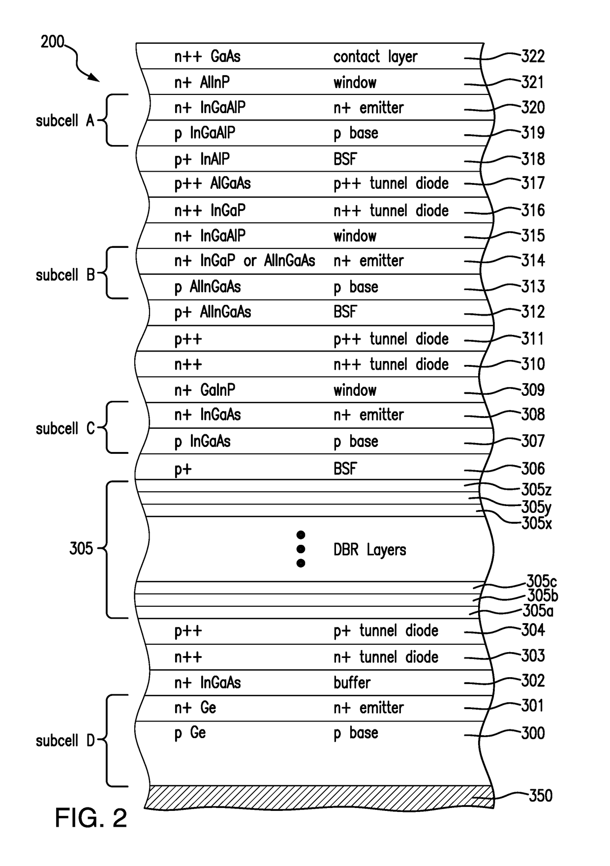
[0148]Turning to the multijunction solar cell device of the present disclosure, FIG. 2 is a cross-sectional view of a four junction solar cell 400 after several stages of fabrication including the growth of certain semiconductor layers on the growth substrate up to the contact layer 322 according to the present disclosure.

[0149]As shown in the illustrated example of FIG. 2, the bottom or fourth subcell D includes a growth substrate 300 formed of p-type germanium (“Ge”) which also serves as a base layer. A back metal contact pad 350 formed on the bottom of base layer 300 provides electrical contact to the multijunction solar cell 200. The bottom subcell D, further includes, for example, a highly doped n-type Ge emitter layer 301, and an n-type indium gallium arsenide (“InGaAs”) nucleation layer 302. The nucleation layer is deposited over the base layer, and the emitter layer is formed in the substrate by diffusion of dopants into the Ge substrate, thereby forming the n-type Ge layer ...

second embodiment

[0172]FIG. 4A is a cross-sectional view of a four junction solar cell 400 after several stages of fabrication including the growth of certain semiconductor layers on the growth substrate up to the contact layer 322, with various subcells being similar to the structure described and depicted in FIG. 2. In the interest of brevity, the description of layers 350, 300 to 304, and 306 through 322 will not be repeated here.

[0173]In the embodiment depicted in FIG. 4A, an intermediate graded interlayer 505, comprising in one embodiment step-graded sublayers 505a through 505z, is disposed over the tunnel diode layer 304. In particular, the graded interlayer provides a transition in the in-plane lattice constant from the lattice constant of the substrate to the larger lattice constant of the middle and upper subcells.

[0174]The graph on the left side of FIG. 4A depicts the in-plane lattice constant being incrementally monotonically increased from sublayer 505a through sublayer 505z, such sublay...

fourth embodiment

[0186]FIG. 5 is a cross-sectional view of a four junction solar cell 500 after several stages of fabrication including the growth of certain semiconductor layers on the growth substrate up to the contact layer 322, with various subcells being similar to the structure described and depicted in FIG. 3.

[0187]In this embodiment, both a grading interlayer 505 and a DBR layer 305 are disposed between subcell C and subcell D. The layers 450, 400 to 404, 504 to 507 and 306 through 322 are substantially similar to that of FIG. 2 and FIG. 4A or 4B and their description need not be repeated here.

[0188]In this embodiment, Distributed Bragg reflector (DBR) layers 305 are then grown adjacent to and over the alpha layer 507 (or the metamorphic buffer layer 505 if layer 507 is not present). The DBR layers 305 are arranged so that light can enter and pass through the third solar subcell C and at least a portion of which can be reflected back into the third solar subcell C by the DBR layers 305. In t...


PUM


Abstract

A four junction solar cell having an upper first solar subcell composed of a semiconductor material having a first band gap; a second solar subcell adjacent to said first solar subcell and composed of a semiconductor material having a second band gap smaller than the first band gap and being lattice matched with the upper first solar subcell; a third solar subcell adjacent to said second solar subcell and composed of a semiconductor material having a third band gap smaller than the second band gap and being lattice matched with the second solar subcell; and a fourth solar subcell adjacent to and lattice mismatched from said third solar subcell and composed of a semiconductor material having a fourth band gap smaller than the third band gap; wherein the fourth subcell has a direct bandgap of greater than 0.75 eV, and the average band gap of the solar cell is equal to or greater than 1.35 eV.

Description

REFERENCE TO RELATED APPLICATIONS[0001]This application is a continuation-in-part of U.S. patent application Ser. No. 14 / 828,206, filed Aug. 17, 2015, which is incorporated herein by reference in its entirety.[0002]This application is related to co-pending U.S. patent application Ser. No. 14 / 660,092 filed Mar. 17, 2015, which is a division of U.S. patent application Ser. No. 12 / 716,814 filed Mar. 3, 2010, now U.S. Pat. No. 9,018,521; which was a continuation in part of U.S. patent application Ser. No. 12 / 337,043 filed Dec. 17, 2008.[0003]This application is also related to co-pending U.S. patent application Ser. No. 13 / 872,663 filed Apr. 29, 2013, which was also a continuation-in-part of application Ser. No. 12 / 337,043, filed Dec. 17, 2008.[0004]This application is also related to U.S. patent application Ser. No. 14 / 828,197, filed Aug. 17, 2015.[0005]All of the above related applications are incorporated herein by reference in their entireties.BACKGROUND OF THE INVENTIONField of the...

Claims


Application Information

Patent Timeline
Patent Type & Authority Applications(United States)
IPC IPC(8): H01L31/041H01L31/0687H01L31/18B64G1/44
CPCH01L31/041H01L31/0687H01L31/1844H01L31/1852B64G1/443Y02E10/544H01L31/048H01L31/0504H01L31/078Y02P70/50
Inventor DERKACS, DANIELBITTNER, ZACHARYWHIPPLE, SAMANTHAHAAS, ALEXANDERHART, JOHNMILLER, NATHANIELPATEL, PRAVINSHARPS, PAUL
Owner SOLAERO TECH CORP
Why Eureka
Try Eureka