HfLaO passivated zinc-oxide thin-film transistor with high field-effect mobility

a thin-film transistor and passivating technology, applied in semiconductor devices, semiconductor/solid-state device details, electrical devices, etc., can solve the problems of high price of igzo tft, achieve low zno tft mobility, reduce moisture absorption, and reduce the amount of unwanted ho—zn—oh compounds

Inactive Publication Date: 2018-11-29
NVMD TECH A CALIFORNIA CORP
View PDF3 Cites 4 Cited by
  • Summary
  • Abstract
  • Description
  • Claims
  • Application Information

AI Technical Summary

Benefits of technology

[0020]In particular, we believe that moisture absorption breaks the Zn—O bonding in ZnO crystals, producing HO—Zn—OH (Zn(OH)2) compounds. These HO—Zn—OH compounds may form dangling bonds and charged scattering centers that strongly lower the mobility of the ZnO TFT.
[0021]It appears that for passivation purposes, LaO-based dielectrics (such as HfLaO) may be superior to other passivation techniques. This is because, according to the XPS data, LaO dielectrics reduce moisture absorption, and thus producing a lower amount of the unwanted HO—Zn—OH compounds.

Problems solved by technology

However, IGZO TFT are expensive because Indium (In) is a rare material, present in only limited quantities in the Earth's crust.

Method used


Image

  • HfLaO passivated zinc-oxide thin-film transistor with high field-effect mobility
  • HfLaO passivated zinc-oxide thin-film transistor with high field-effect mobility
  • HfLaO passivated zinc-oxide thin-film transistor with high field-effect mobility

Examples


Embodiment Construction

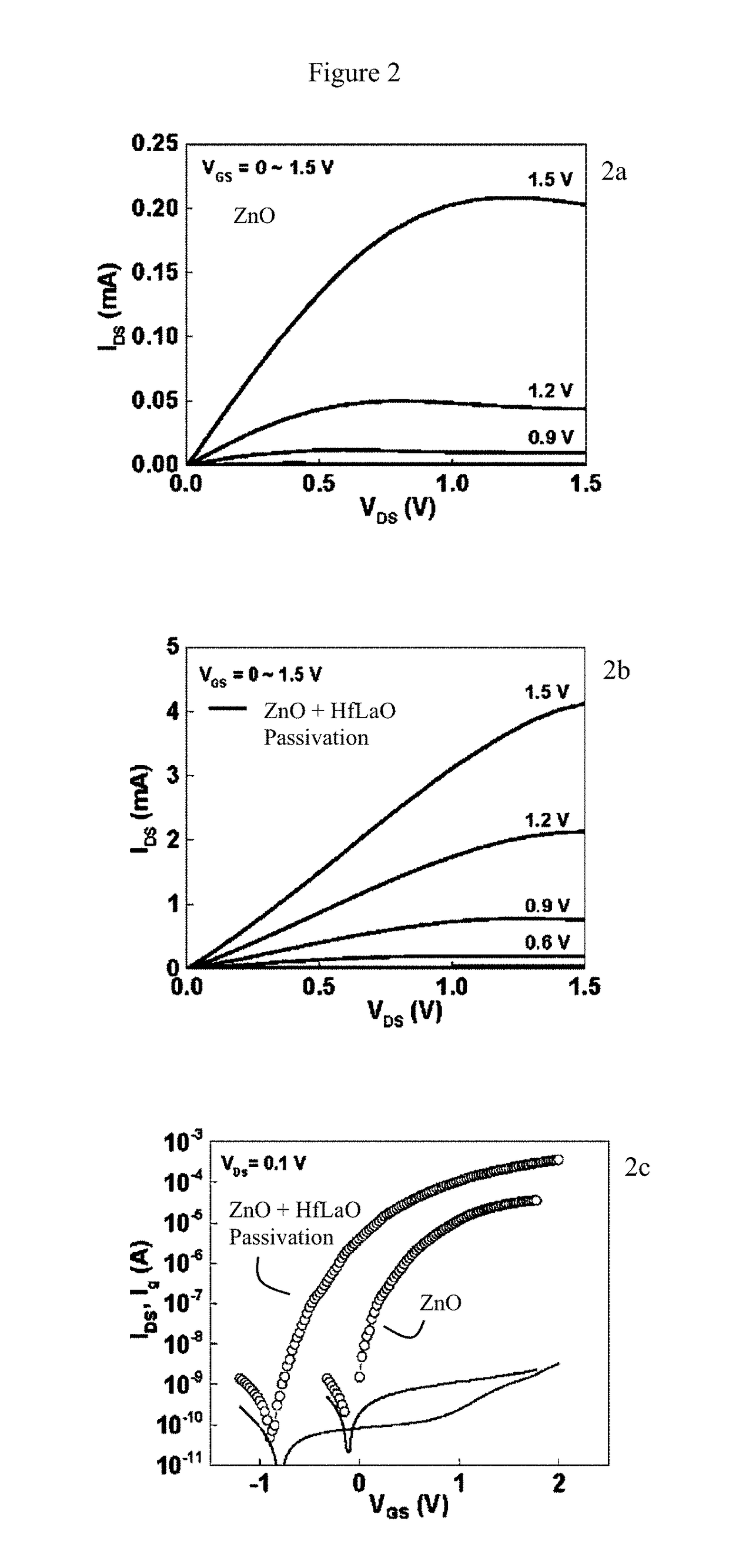
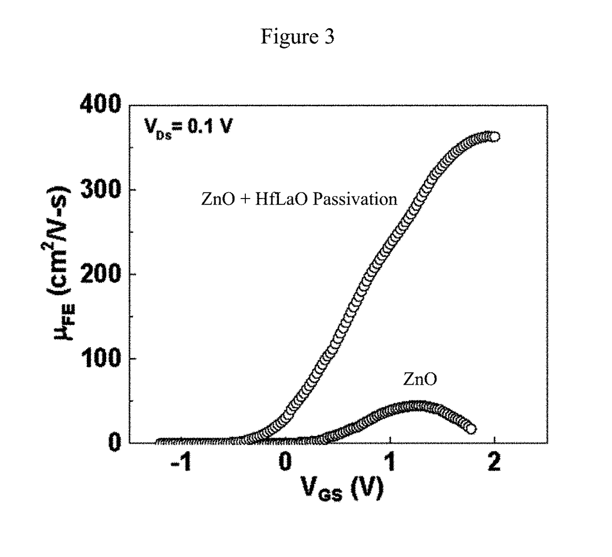
[0029]As previously discussed, the invention may be viewed as a solution to the problem, “Why do ZnO based TFT have generally unimpressive performance?”, or “How to produce ZnO based TFT with substantially improved performance?”

[0030]As will be described in more detail shortly, in one embodiment, the invention may be an apparatus (e.g. an electronic apparatus) comprising: a flexible (e.g. PEN) or a rigid (e.g. glass) substrate layer, with at least one multi-layer thin-film transistor disposed over this substrate layer. At least one of these layers will comprise a nano-crystalline zinc-oxide metal-oxide channel layer. In some embodiments, other types of metal oxide channel layers may also be used. At least some of these layers will further comprise gate layers. In a particularly favored embodiment, at least one of these layers will further comprise an HfLaO passivation layer selected to prevent ambient moisture from disrupting nano-crystals in the nano-crystalline zinc-oxide channel ...


PUM


Abstract

Improved thin film transistor device and method, comprising transparent multi-layer thin-film transistors (TFT) disposed over a flexible polyethylene naphthalate (PEN) substrate with a nano-crystalline ZnO channel layer, and a novel HfLaO passivation layer. This device, which may be made at room temperature, has a high field-effect mobility (μFE) of 345 cm2/Vs, small sub-threshold slope (SS) of 103 mV/dec, high on-current/off-current (ION/IOFF) of 7×10⁶, and a low drain-voltage (VD) of 2V for low power operation. Although prior art ZnO based TFT had unimpressive performance, use of the novel HfLaO passivation layer appears to greatly improve the performance of ZnO TFT by preventing trace levels of H2O from forming unwanted Zn—OH bonds, thus disrupting ZnO nanocrystals. At least some of the problems with prior ZnO TFT may be attributed to these Zn—OH bonds, which damage ZnO crystallinity, create charged scattering centers, and form potential barriers that degrade mobility.

Description

BACKGROUND OF THE INVENTIONField of the Invention[0001]This invention is in the field of thin film transistors and semiconductor passivation technology.Description of the Related Art[0002]Thin film transistors (TFT) are a type of field effect transistor. TFT are multi-layered devices, typically formed from thin films of active semiconductors on a supporting substrate. This substrate can be a rigid substrate, such as glass, or a flexible substrate such as Polyethylene naphthalate (PEN). Thin film transistors typically also use transparent electrodes formed from various materials such as indium tin oxide (ITO) and other materials.[0003]The various TFT thin films can be made to be transparent, and the TFT substrate, regardless of if it is rigid or flexible, can also be transparent, thus creating a transparent device. As a result thin film transistors can be useful for various display devices such as liquid crystal displays (LCD) and the like.[0004]High field effect mobility (μF) is con...

Claims


Application Information

Patent Timeline
Patent Type & Authority Applications(United States)
IPC IPC(8): H01L29/786H01L29/04H01L23/31H01L23/29H01L21/56
CPCH01L29/7869H01L29/78603H01L29/04H01L23/3171H01L29/4908H01L29/78606H01L29/78636H01L21/56H01L29/45H01L23/291H01L27/1248
Inventor CHIN, ALBERT
Owner NVMD TECH A CALIFORNIA CORP
Why Eureka
Try Eureka