
Solder alloy, solder ball, and solder joint

a solder ball and alloy technology, applied in the direction of soldering apparatus, manufacturing tools, welding/cutting media/materials, etc., can solve the problems of forming vacancies in the cathode-side portion of the solder joint, the current density per terminal of the semiconductor elements mounted on such electronic devices becomes higher, and the solder joint ruptures. , to achieve the effect of high bonding strength, inhibiting em, and high wetting properties

Active Publication Date: 2018-12-20
SENJU METAL IND CO LTD
View PDF6 Cites 4 Cited by
  • Summary
  • Abstract
  • Description
  • Claims
  • Application Information

AI Technical Summary

Benefits of technology

This patent describes a method for improving the properties of a solder alloy used in electronic devices. The inventors found that adding specific elements to the alloy can enhance its ability to wet surfaces and bond materials together. By controlling the ratio between these elements, they were able to prevent the formation of electromagnetic interference (EMI). The patent also mentions that adding certain other elements, such as iron or phosphorus, can further improve the alloy's bonding strength and prevent the formation of voids at the bonding interfaces. Overall, the inventors found that a combination of elements and their contents can have a significant impact on the properties of the solder alloy.

Problems solved by technology

This has resulted in a tendency that the current density per terminal of the semiconductor elements mounted on such electronic devices becomes higher.
The progress of the electromigration may result in ruptures of the solder joints.
The movement of the atoms toward the anode side of the solder joint results in the formation of vacancies in a cathode-side portion of the solder joint.
The formed voids grow to finally cause a rupture of the solder joint.
Because of the recent increases in current density, EM is becoming a serious problem.
These solder alloys are prone to suffer EM because Sn, which is used therein as a main component, has a large number of net charges.
There are cases where solder joints formed from these alloys rupture when a current is caused to flow therethrough at a high current density over a long period.

Method used

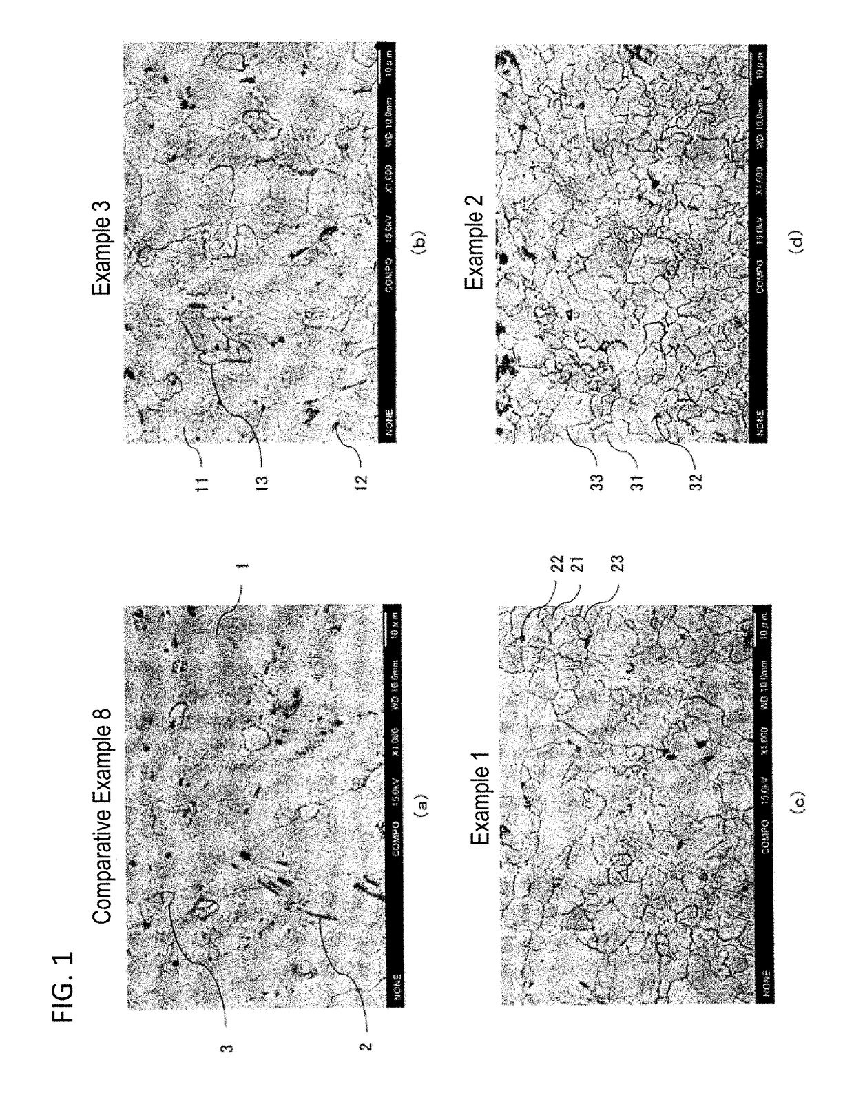
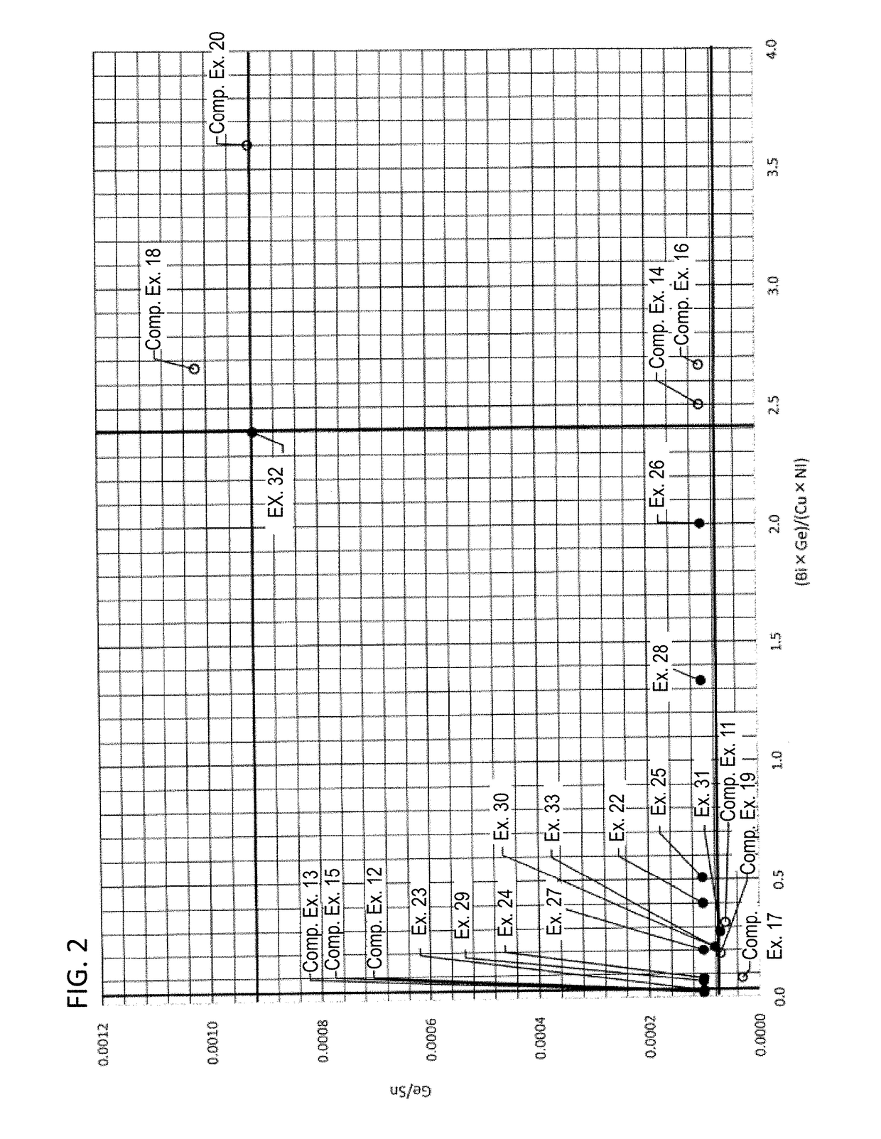
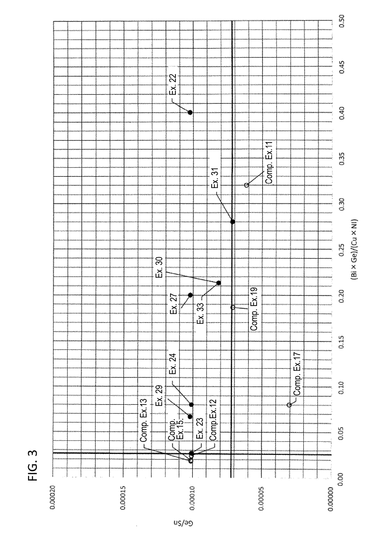

Image

  • Solder alloy, solder ball, and solder joint
  • Solder alloy, solder ball, and solder joint
  • Solder alloy, solder ball, and solder joint

Examples


examples

[0087]Solder alloys respectively consisting of the alloy compositions shown in Tables 1 and 2 were used to form solder joints. The solder joints formed were evaluated for bonding strength by conducting a shear strength test, examination of rupture M, and EM test. The solder alloys were evaluated also for wetting property. The evaluation methods used are as follows.

[0088]Shear Strength

[0089]Soldering was conducted as follows: the solder alloys shown in Tables 1 and 2 were each bonded to OSP-treated Cu electrodes (hereinafter referred to simply as “Cu electrodes”) of a PCB having a substrate thickness of 1.2 mm and an electrode size of 0.24 mm in diameter. The soldering was conducted in the following manner: solder balls having a diameter of 0.3 mm were produced beforehand from each solder alloy; a water-soluble flux (WF-6400, manufactured by Senju Metal Industry Co., Ltd.) was applied to the substrate, and the balls were then placed thereon; and thereafter, soldering was performed by...


PUM

PropertyMeasurementUnit
compositionaaaaaaaaaa
current densityaaaaaaaaaa
massaaaaaaaaaa

Abstract

A solder alloy has an alloy composition consisting of, in mass %: Bi: 0.1% or more and less than 2.0%, Cu: 0.1 to 1.0%, Ni: 0.01 to 0.20%, Ge: 0.006 to 0.09%, and Co: 0.003% or more and less than 0.05%, and optionally Fe: 0.005 to 0.015% and P: 0.1% or less, with the balance being Sn.

Description

CROSS-REFERENCE TO RELATED PATENT APPLICATIONS[0001]This application is a U.S. National Phase Application under 35 U.S.C. § 371 of International Patent Application No. PCT / JP2017 / 032834 filed on Sep. 12, 2017 and claims the benefit of Japanese Patent Applications No. 2016-178879, filed on Sep. 13, 2016, and No. 2016-178880, filed on Sep. 13, 2016, all of which are incorporated herein by reference in their entireties. The International Application was published in Japanese on Mar. 22, 2018 as International Publication No. WO / 2018 / 051973 under PCT Article 21(2).FIELD OF THE INVENTION[0002]The present invention relates to a solder alloy through which a current can be caused to flow at a high current density, and to a solder ball and a solder joint.BACKGROUND OF THE INVENTION[0003]Electronic devices having solder joints, such as CPUs (central processing units), have recently come to be required to have smaller sizes and higher performances. This has resulted in a tendency that the curre...

Claims


Application Information

Patent Timeline
Patent Type & Authority Applications(United States)
IPC IPC(8): B23K35/26B23K35/02C22C13/02C22C13/00
CPCB23K35/262B23K35/0244C22C13/02C22C13/00H05K3/3457H05K3/3463
Inventor TACHIBANA, KENNOMURA, HIKARUIIJIMA, YUKIYOSHIKAWA, SHUNSAKUIZUMITA, NAOKOSAITO, TAKASHIYOKOYAMA, TAKAHIRO
Owner SENJU METAL IND CO LTD
Learn More