Multi-well selenium device and method for fabrication thereof

a selenium device and multi-well technology, applied in the direction of radiation control devices, diodes, semiconductor devices, etc., can solve the problems of avalanche-mode selenium not being the bulk medium, unable to be used as photon-counting mode detection, and variable dependent gain

Active Publication Date: 2019-01-03
THE RES FOUND OF STATE UNIV OF NEW YORK
View PDF0 Cites 16 Cited by
  • Summary
  • Abstract
  • Description
  • Claims
  • Application Information

AI Technical Summary

Benefits of technology

[0018]To overcome shortcomings of conventional systems, a multi-well selenium detector provided herein and a method for the fabrication of same that eliminates the required alignment and encapsulates grid electrodes with the insulator / dielectric.

Problems solved by technology

Disordered solids, which are easier and less expensive to develop than single crystalline solids, have not been utilized as photon-counting mode detection media because of low carrier mobility and transit-time-limited photo response.
For high-energy penetrating radiation, the challenge is that avalanche-mode selenium cannot be the bulk medium because avalanche layers cannot be very thick (<25 μm) and a uniform avalanche field in the bulk causes depth-dependent gain variations.
Without the TOF localization data, computationally expensive iterative reconstruction algorithms are used to estimate the 3D distribution of events that provide the best match with the measured projection data.
However, this goals has not been realized.
Existing systems utilize expensive photomultiplier tubes (PMTs) that are based on the complicated plano-concave photocathode, yet can only achieve Δt of ˜500 ps.
However, SiPMs suffer from poor photon detection efficiency, optical crosstalk, small area, poor uniformity, and high cost.
However, such direct conversion a-Se FPD has not been realized due to formation of field hot-spots, where the applied electric field (F) exceeds 150 Wm, which lead to irreversible material breakdown.
Limitations of direct conversion a-Se FPDs include degradation of low-dose imaging performance due to electronic noise since the energy required to generate an electron-hole pair in a-Se is 50 eV at 10 V / micron.
Although other photoconductive materials with higher conversion have been investigated, direct conversion a-Se FPDs remain far from commercialization due to charge trapping and manufacturing issues.
However, this electric field increase is extremely challenging for reliable detector construction and operation, and is impractical.
Amorphous solids, i.e., non-crystalline solids with disorder, have been ruled out as viable radiation imaging detectors in a photon-counting mode because of low temporal resolution due to low carrier mobilities and transit-time limited pulse response, and low conversion gain of high energy radiation to electric charge.
A direct conversion a-Se layer with separate absorption and avalanche region has been suggested, but significant obstacles prevent practical implementation of a direct conversion a-Se layer with separate absorption and avalanche regions.
[11-13] However, such detector structures are not practical for direct conversion avalanche gain because the highest electric field in the well develops at the interface between the semiconductor and the pixel electrode, resulting in a high dark current due to large charge injection and potentially irreversible damage to the detector.
[12,13,15-17] However, conventional systems do not etch dielectric at the bottom of wells, nor are grid electrodes encapsulated with dielectric layers provide on each side thereof.
[15, 16] However, these methods require alignment, i.e., alignment during lithography, for encapsulating the grid electrodes with insulator / dielectric while removing the insulator / dielectric at the bottom of the wells.

Method used


Image

  • Multi-well selenium device and method for fabrication thereof
  • Multi-well selenium device and method for fabrication thereof
  • Multi-well selenium device and method for fabrication thereof

Examples


Embodiment Construction

[0031]The following detailed description of certain embodiments of the present invention will be made with reference to the accompanying drawings. In describing the invention, explanation about related functions or constructions known in the art are omitted for the sake of clearness in understanding the concept of the invention, to avoid obscuring the invention with unnecessary detail.

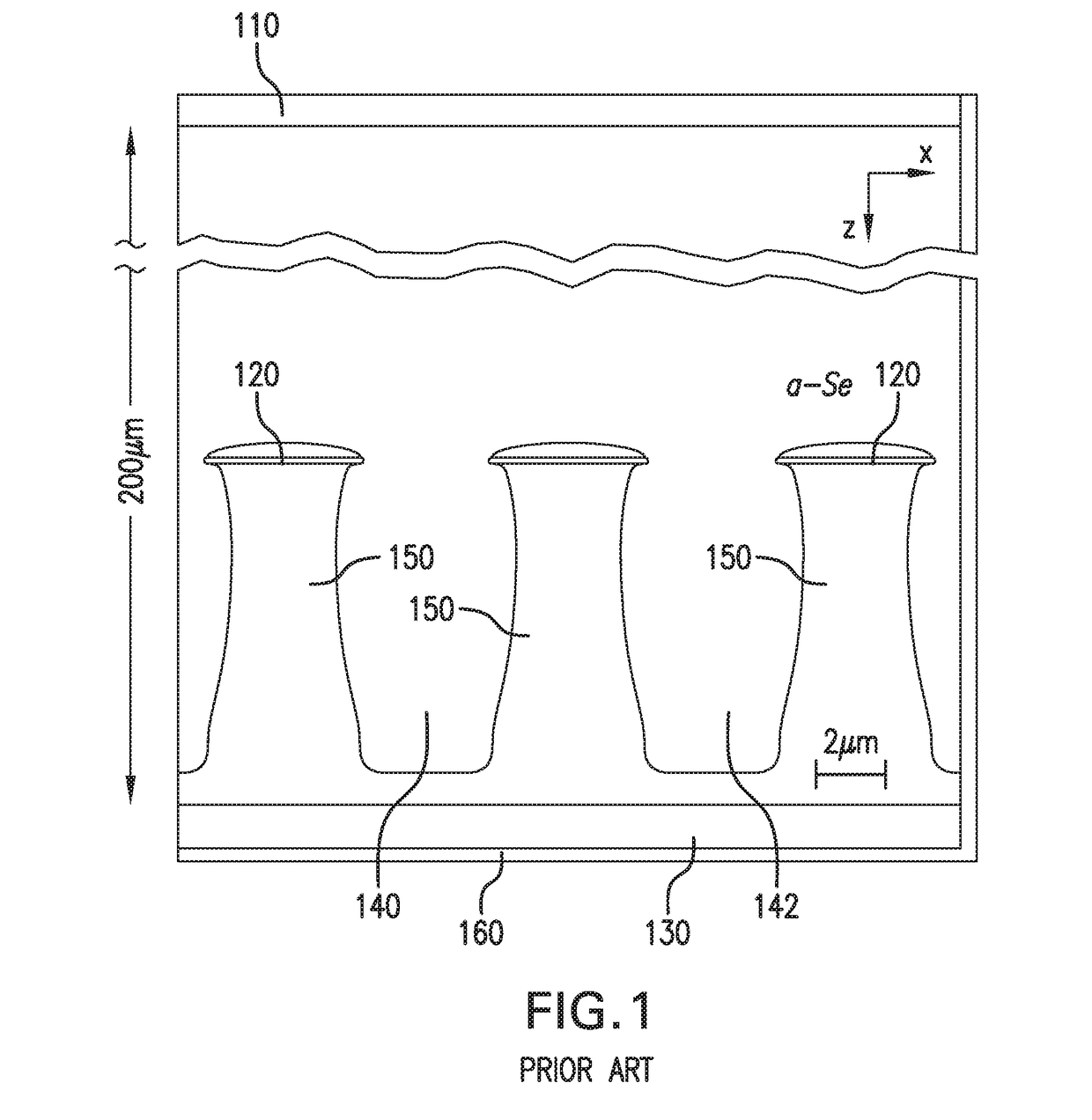
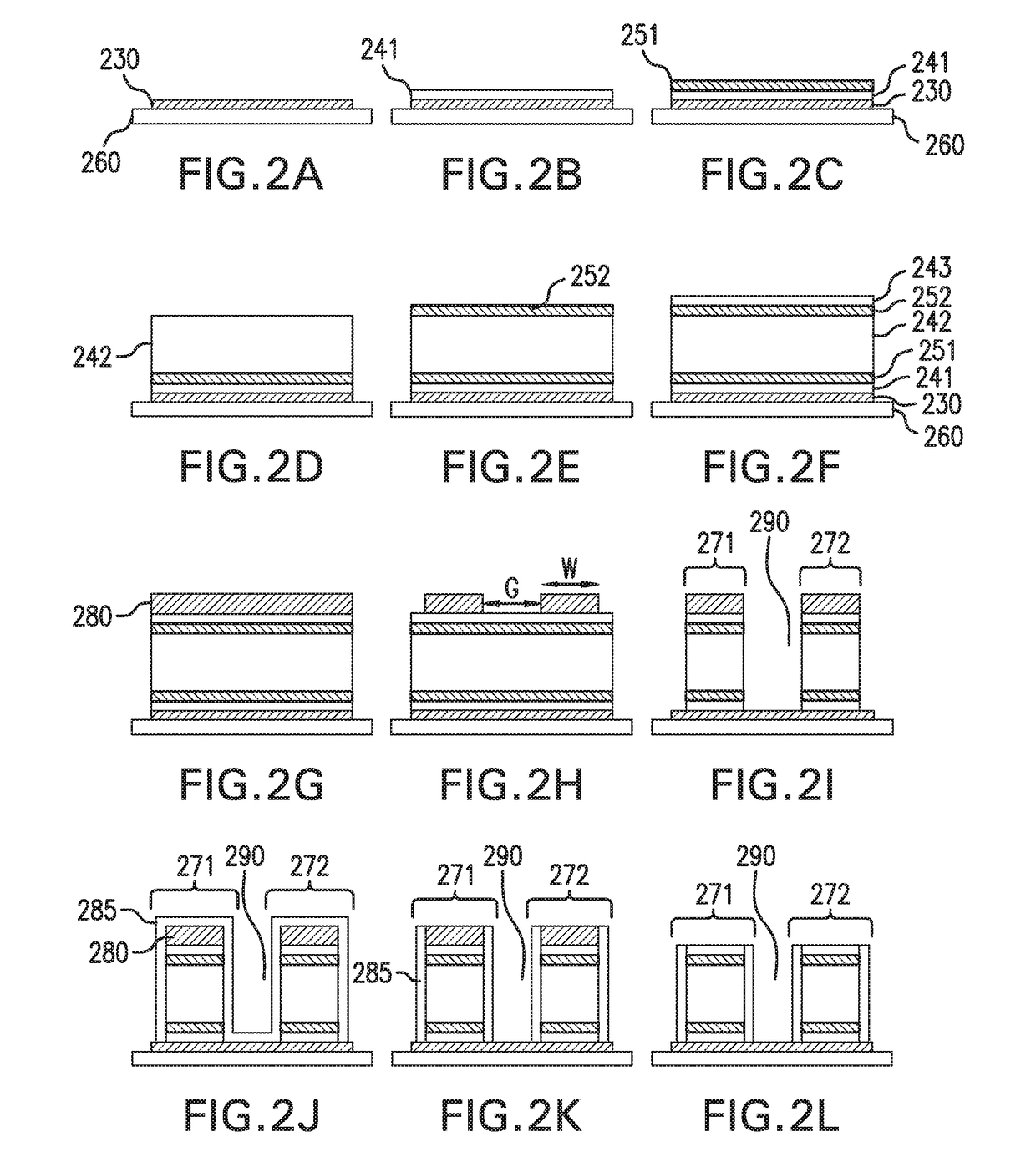
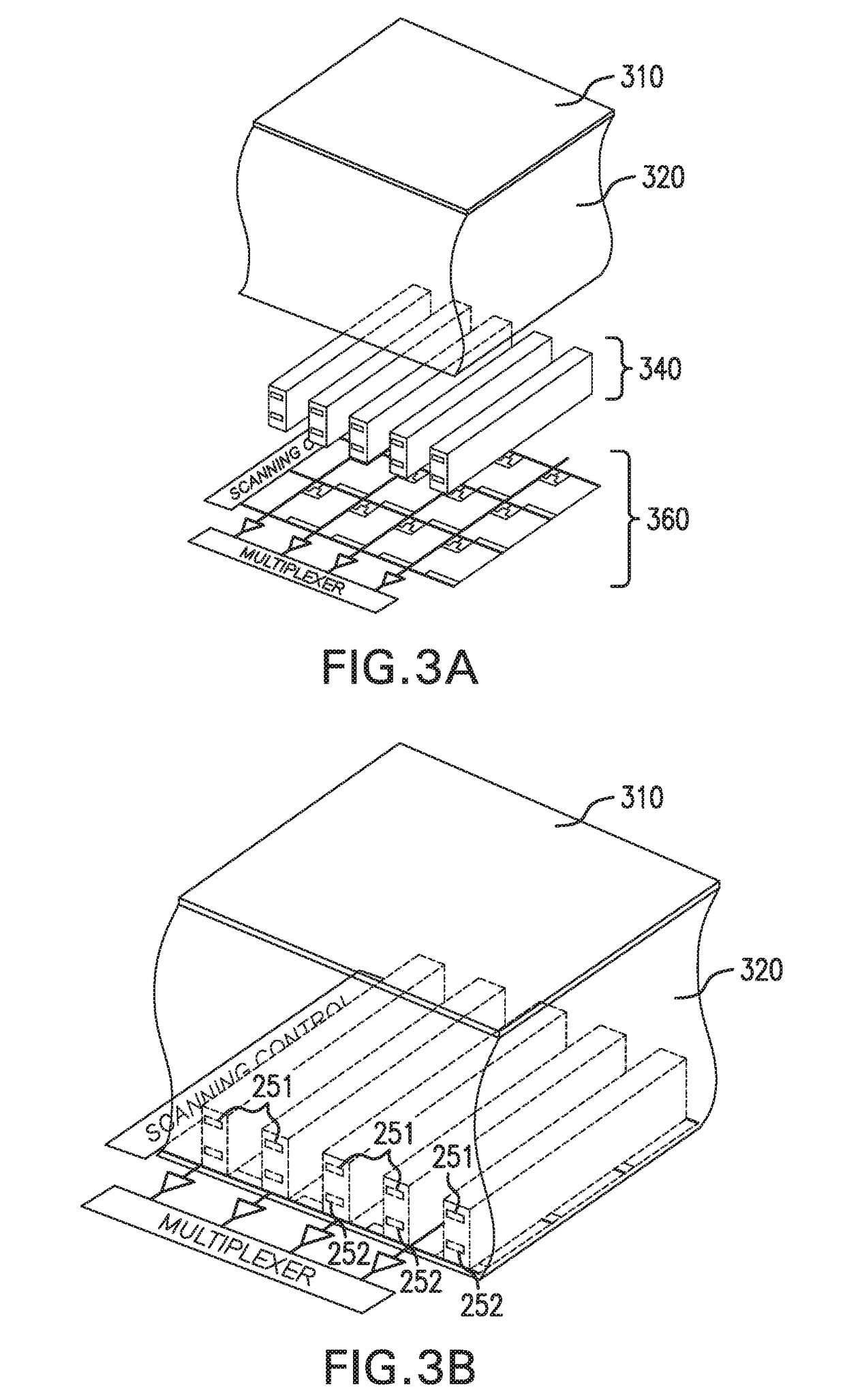
[0032]Disclosed herein is a solid-state avalanche radiation detector, and a method for constructing same, using amorphous material as the photoconductive layer without field hot-spots, to provide a direct conversion avalanche a-Se. The solid-state avalanche radiation detector is based on field-shaping by localizing the high-field avalanche region between two low-field regions, improving on the devices of Sauli, Lee, and Goldan. [9, 11, 14-16]

[0033]The present disclosure optimizes the solid-state detector structure to provide stable avalanche multiplication gain in direct conversion amorphous selenium r...


PUM


Abstract

Provided is a field shaping multi-well detector and method of fabrication thereof. The detector is configured by depositing a pixel electrode on a substrate, depositing a first dielectric layer, depositing a first conductive grid electrode layer on the first dielectric layer, depositing a second dielectric layer on the first conductive grid electrode layer, depositing a second conductive grid electrode layer on the second dielectric layer, depositing a third dielectric layer on the second conductive grid electrode layer, depositing an etch mask on the third dielectric layer. Two pillars are formed by etching the third dielectric layer, the second conductive grid electrode layer, the second dielectric layer, the first conductive grid electrode layer, and the first dielectric layer. A well between the two pillars is formed by etching to the pixel electrode, without etching the pixel electrode, and the well is filled with a-Se.

Description

PRIORITY[0001]This application claims priority to U.S. Provisional Patent Application No. 62 / 275,919 filed with the U.S. Patent and Trademark Office on Jan. 7, 2016, the entire contents of which is incorporated herein by reference.GOVERNMENT SUPPORT[0002]This invention was made with government support under grant number 1R21 EB01952601A 1 awarded by the National Institute of Health. The government has certain rights in the invention.BACKGROUND OF THE INVENTION1. Field of the Invention[0003]The present invention relates generally to the field of solid-state radiation imaging detectors and, in particular, to amorphous selenium radiation detectors having a field-shaping multi-well detector structure.2. Description of the Related Art[0004]Soon after the Nobel Prize winning invention of the gas-filled multi-wire proportional chamber by Charpak in 1968, and parallel to developments in microelectronics, micro-pattern gaseous detectors were developed for improved position resolution. Howeve...

Claims


Application Information

Patent Timeline
Patent Type & Authority Applications(United States)
IPC IPC(8): H01L31/0272H01L31/0376H01L31/0224H01L31/0216H01L27/146H01L31/107H01L31/105
CPCH01L31/0272H01L31/0376H01L31/022408H01L31/02161H01L27/14643H01L31/107H01L27/14692H01L31/105H01L27/1461H01L27/14612H01L27/1463H01L27/14632H01L27/14636H01L27/14659H01L27/14696H01L31/035209H01L27/14634H01L27/14665H01L31/0224H01L31/0392H01L31/08
Inventor GOLDAN, AMIRHOSSEINZHAO, WEI
Owner THE RES FOUND OF STATE UNIV OF NEW YORK
Why Eureka
Try Eureka