Supercharge Your Innovation With Domain-Expert AI Agents!

Chemical vapor deposition of perovskite thin films

a technology of perovskite and vapor deposition, which is applied in the direction of electrical equipment, coatings, metal material coating processes, etc., can solve the problems of toxicity due to the presence, preventing the commercialization of such solar cells, and challenging the possibility of further scaling up and eventual commercialization

Active Publication Date: 2019-03-07
WASHINGTON UNIV IN SAINT LOUIS
View PDF0 Cites 11 Cited by
  • Summary
  • Abstract
  • Description
  • Claims
  • Application Information

AI Technical Summary

Benefits of technology

The patent text describes a new device called a memristor that uses a perovskite film to change its resistance. The device can be made using a chemical vapor deposition method, where different precursors are mixed and then deposited onto a substrate to create the perovskite film. The resulting film has unique properties that make it useful in a variety of applications, such as resistive switching memory devices. Overall, this technology allows for the creation of highly precise and reliable resistance change devices that can perform valuable functions in the field of electronics.

Problems solved by technology

Though the reported power conversion efficiencies of lead halide perovskite solar cells are now competitive with commercial silicon solar cells, there are two limitations preventing the commercialization of such solar cells.
These are (1) the environmental, device and thermodynamic instability of the perovskites in the presence of air, humidity, light and electric fields; and (2), the toxicity due to the presence of lead.
However, the toxicity due to the presence of lead in these perovskites presents a challenge to further scale-up and eventual commercialization.
Reports on optoelectronic and photovoltaic properties of methylammonium bismuth iodide (CH3NH3)3Bi2I9 (MA3Bi2I9) with high absorption coefficient and long term stability have been published; however, MA3Bi2I9 based solar cells suffer from low efficiency.
Besides the sub-optimal electronic structure of MA3Bi2I9 compared to MAPbI3, the diminished performance of the solar-cells is also attributed to the commonly used solution deposition techniques that result in poor morphology, purity and coverage of the films on substrate.
However, so far, bismuth-based halide materials have been rarely reported to fabricate resistive switching memories, only two types of bismuth-based halide films have been demonstrated memristive performance.
Furthermore, their performances, such as ON / OFF ratios (3), are still not comparable to that of a MAPbI3 based memory device.
More fundamentally, the nature of resistive switching behavior in bismuth-based halide perovskite memory devices has not been clarified yet.
But, oxide-based inorganic perovskites rely on high-temperature vacuum-based deposition synthesis (>450° C.) and form brittle rigid films, thus limiting their application to rigid substrates.
However, future technologies including ubiquitous electronics and the Internet of Things (IoT) require flexible devices fabricated on soft substrates, which are usually unstable at high temperature.
Nevertheless, the toxicity of lead as well as the instability of MAPbI3 in the presence of moisture and oxygen restricts the further scale-up and commercialization.

Method used


Image

  • Chemical vapor deposition of perovskite thin films
  • Chemical vapor deposition of perovskite thin films
  • Chemical vapor deposition of perovskite thin films

Examples


examples

[0070]Preparation of Methylammonium Iodide (MAI)

[0071]25 mL of methylamine (33 wt % in ethanol) was added to a 250 mL, three-neck flask at a temperature below 7° C. 10 mL of hydroiodic acid (HI, 57 wt % in water) was added to the MAI solution while stirring. The MAI precipitate was recovered under reduced pressure and a water bath temperature below 50° C.

[0072]The MAI was recrystallized three times in absolute ethanol and diethyl ether. A white powder was obtained and dried at 60° C. overnight under vacuum. The phase purity of the compound was confirmed by a powder X-ray diffractometer (FIG. 9).

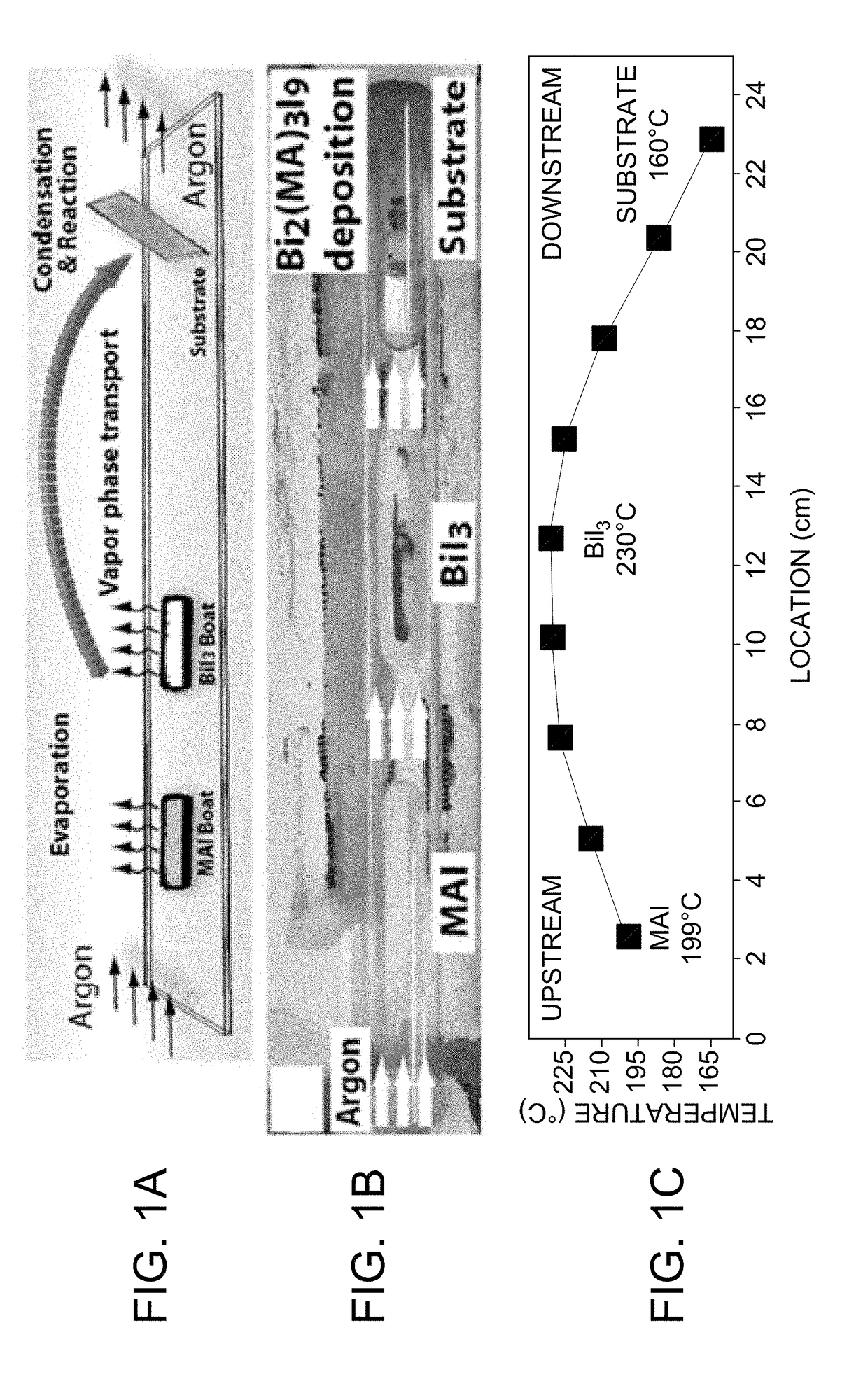
[0073]Perovskite Synthesis Via APCVD

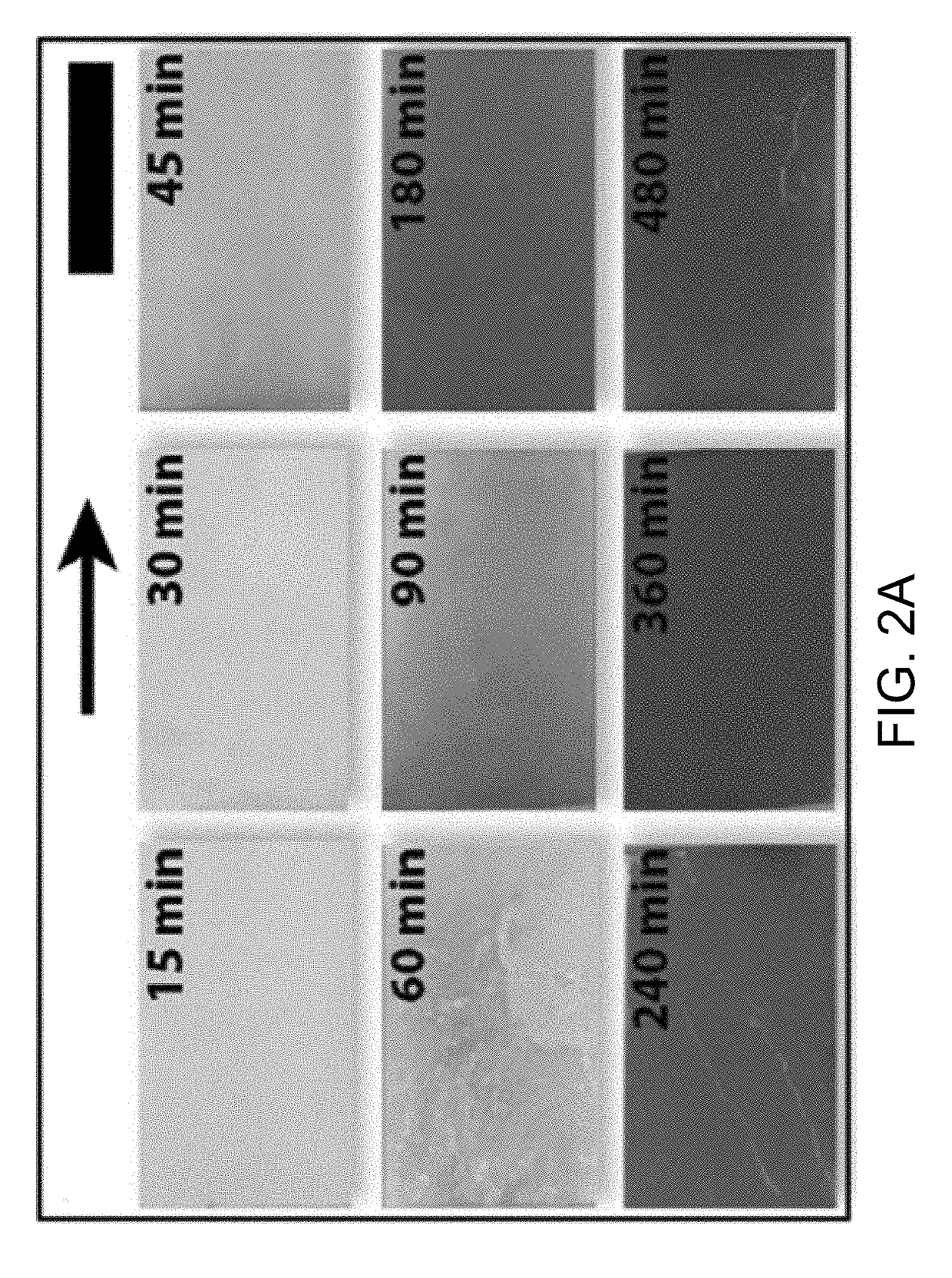
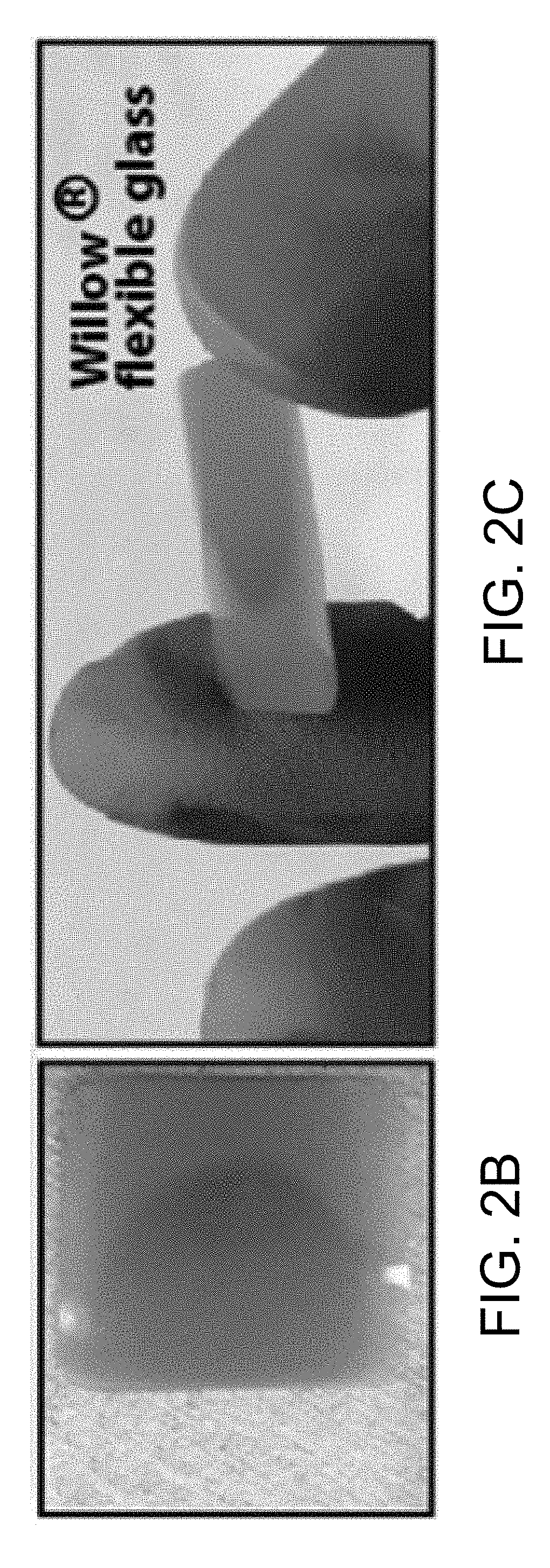
[0074]The MAI prepared above was used as a first precursor for the APCVD, and BiI3 (99%) was used as a second precursor. A quartz tube mounted on a single zone furnace was used for the APCVD studies. Silicon wafers (Test Grade) with or without a 100 nm thermal oxide layer, glass slides, pre-cut 5 mm×5 mm high purity quartz substrates and 2 cm×2 cm WILLOW® f...


PUM

PropertyMeasurementUnit
Electric potential / voltageaaaaaaaaaa
Temperatureaaaaaaaaaa

Abstract

Perovskite films are known to be useful in many different technologies, including solar panels and memristors. Most perovskites contain lead which is undesirable for many reasons. It has been found that bismuth can be used in place of lead in preparing perovskite thin films. Additionally, when chemical vapor deposition is used to prepare the films instead of traditional solution phase methods, the films show greatly improved performance in electronic applications. Additionally, the present disclosure is directed to the use of perovskites in memory devices.

Description

CROSS-REFERENCE TO RELATED APPLICATION[0001]This application claims the benefit of U.S. Provisional Patent Application Ser. No. 62 / 550,222, filed Aug. 25, 2017, the entire contents of which are incorporated herein by reference.STATEMENT REGARDING FEDERALLY SPONSORED RESEARCH & DEVELOPMENT[0002]This invention was made with government support under grant DE-AC36-08GO28308 awarded by Office of Science, Office of Basic Energy Sciences, and Energy Efficiency and Renewable Energy, Solar Energy Technology Program, grant IUSSTF / JCERDC-SERIIUS / 2012 awarded by Department of Science and Technology, Government of India, grant W911NF-15-1-0178, subgrant RSC15032 awarded by U.S. Army RDECOM, and grant number ACI-1053575 awarded by the National Science Foundation. The government has certain rights in the invention.BACKGROUND[0003]The field of the disclosure relates generally to the formation of perovskite thin films using bismuth instead of lead. It discloses the use of chemical vapor deposition t...

Claims


Application Information

Patent Timeline
IPC IPC(8): H01L45/00
CPCH01L45/14H01L45/1616C23C16/30H10N70/881H10N70/023
Inventor BANERJEE, PARAGCHENG, PEIFUCHEN, XIAOMYUNG, YOON
Owner WASHINGTON UNIV IN SAINT LOUIS
Features
  • R&D
  • Intellectual Property
  • Life Sciences
  • Materials
  • Tech Scout
  • Unparalleled Data Quality
  • Higher Quality Content
  • 60% Fewer Hallucinations
Learn More