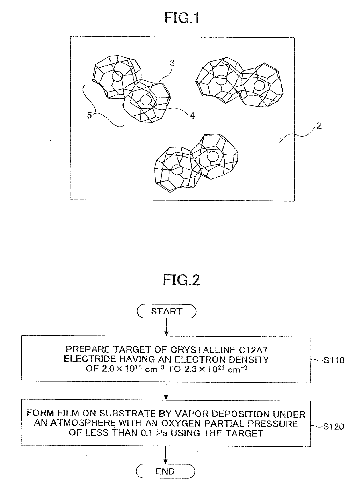
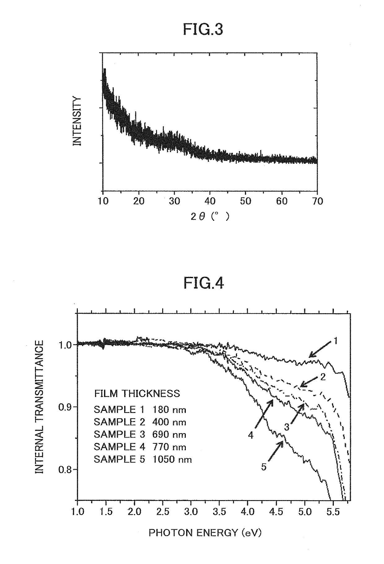
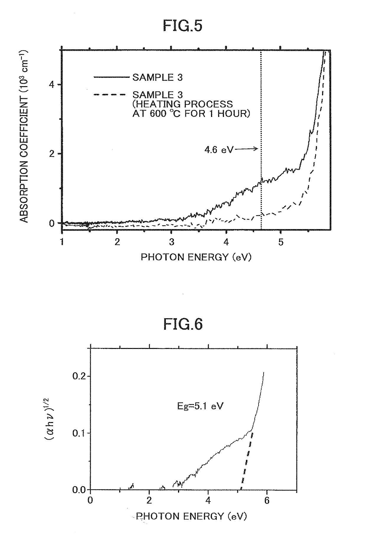
Metal oxide thin film, organic electroluminescence element including the thin film, solar cell, and thin film fabrication method
a technology of metal oxide and thin film, applied in the field of c1, can solve the problem that the method is not suitable for fabricating a crystalline c12a7 electride thin film
- Summary
- Abstract
- Description
- Claims
- Application Information
AI Technical Summary
Benefits of technology
Problems solved by technology
Method used
Image
Examples
example 1
(Target Fabrication)
[0131]First, a raw material powder was obtained by preparing and mixing CaO powder and Al2O3 powder to a molar ratio of 12:7. The raw material powder was heated to 1350° C. in air to fabricate a bulk of crystalline C12A7.
[0132]Then, the crystalline C12A7 bulk was pulverized into powder, and the powder was press-molded through cold isostatic pressing to obtain a crystalline C12A7 molded body. Further, the molded body was placed in a carbon crucible together with metal aluminum and heated to in a vacuum furnace. In the carbon crucible, the molded body and the metal aluminum were separately held. The temperature was heated to 1300° C. and held for 6 hours, and in this way, a crystalline C12A7 electride sintered body was obtained.
[0133]The sintered body was then cut into a disk shape with a thickness of 5 nm and a diameter of 3 inches, and the disk-shaped sintered body was fixed to a Cu backing plate using In to obtain a sputtering target (simply referred to as “targ...
example 2
[0164]Sample 6 was fabricated by forming an amorphous C12A7 electride thin film on a substrate in the same manner as the above Example 1. However, in Example 2, the pre-sputtering process using He gas was not conducted. Instead, before using the crystalline C12A7 electride target, the surface of the crystalline C12A7 electride target was polished with a diamond file. Note that the sputtering process using Ar gas was conducted for 2 hours in the present example. Other processing conditions were the same as those used for fabricating Sample 1 of Example 1.
[0165]FIG. 7 illustrates internal transmittance measurement results of Sample 6. Note that in FIG. 7, the internal transmittance measurement results of Sample 2 is indicated along with the internal transmittance measurement results of Sample 6.
[0166]As can be appreciated from FIG. 7, a substantial decrease in transmittance could be observed in Sample 6 at the position of the photon energy of 4.6 eV.
[0167]Thus, it could be confirmed t...
example 3
[0168](Work Function of Amorphous C12A7 Electride Thin Film)
[0169]A sample (Sample 7) having an amorphous C12A7 electride thin film with a thickness of 10 nm formed on an ITO was fabricated by performing the sputtering process for 4 minutes using a glass substrate with ITO (indium tin oxide) instead of a silica glass substrate. Note that other than the above processing conditions, Sample 7 was fabricated in the same mariner as Example 1.
[0170]The work function of Sample 7 was measured by ultraviolet photoelectron spectroscopy. In order to obtain a clean surface, measurement was performed under ultra-high vacuum (10−7 Pa), and organic matter was removed from the surface by Ar sputtering before measurement. Also, X-ray photoelectron spectroscopy was performed before and after the Ar sputtering process to confirm that the thin film sample has riot been damaged. Further, a DC voltage (bias voltage) was applied to Sample 7 so that Sample 7 may be at a negative potential with respect to t...
PUM
| Property | Measurement | Unit |
|---|---|---|
| work function | aaaaa | aaaaa |
| sintering | aaaaa | aaaaa |
| temperature limit | aaaaa | aaaaa |
Abstract
Description
Claims
Application Information
 - R&D
- Intellectual Property
- Life Sciences
- Materials
- Tech Scout
- Unparalleled Data Quality
- Higher Quality Content
- 60% Fewer Hallucinations
Browse by: Latest US Patents, China's latest patents, Technical Efficacy Thesaurus, Application Domain, Technology Topic, Popular Technical Reports.
© 2025 PatSnap. All rights reserved.Legal|Privacy policy|Modern Slavery Act Transparency Statement|Sitemap|About US| Contact US: help@patsnap.com


