Infra-red devices

a technology of infra-red devices and micro-machined thermal infrared, which is applied in the manufacture/treatment of thermoelectric devices, radiofrequency controlled devices, instruments, etc., can solve the problems of insufficient emissivity, small control of emission at specific wavelengths, and inability to electro-migrate metal layers, etc., to improve the overall ir device array lifetime, reduce thermal dissipation, and improve the overall ir device array performance

Active Publication Date: 2019-10-03
CAMBRIDGE GAN DEVICES LIMITED
View PDF4 Cites 1 Cited by
  • Summary
  • Abstract
  • Description
  • Claims
  • Application Information

AI Technical Summary

Benefits of technology

[0038]According to another embodiment of the present disclosure, there is provided a micromachined AlGaN/GaN-based IR device, wherein the element formed within the membrane region and comprising a 2DEG may be a plasmonic element or a tunable plasmonic element, and wherein the AlGaN/GaN-based IR device is 3D stack on a second IR device. The second IR device may be any of the devices previously disclosed or any other IR device, even realised in a different technology (e.g. a CMOS IR emitter or a CMOS IR detector), in order to provide the second IR device with optical properties different from its native ones. The stacking process may take place at wafer level and may allow the creation of a cavity at low pressure (lower than ambient pressure), in order to reduce thermal dissipation and thus improve the second IR device performance.
[0039]In another embodiment of the disclosure, the heterostructure-based IR device comprises an array of several membranes, wherein each membrane may comprise a previously disclosed element (i.e. a heating element, a temperature sensing element, a plasmonic element and a tunable plasmonic element) or a combination of those. The devices may be the same or different across the array. For example heterostructure-based IR device may comprise an array of heating elements, or in an array of temperature sensing elements, configured respectively to operate as an array of IR emitters or as an array of IR detectors. Each IR device within the array of IR devices may have the same design, wherein such redundancy may improve the overall IR device array lifetime, or each IR device within the array of IR devices may have the different design. For example in case the array of IR devices is an array of IR emitters with tailored optical properties, wherein each IR emitter may be design to emit IR radiation in a specific wavelength region, thus the array of IR emitters with tailored optical properties may be used for spectroscopic analysis. In another example, the array of IR devices is an array of IR detectors with tailored optical properties, wherein each IR detector may be design to detect IR radiation in a specific wavelength region, thus the array of IR detectors with t

Problems solved by technology

One limitation of many of these devices is that their emissivity is not optimal and specifically for the emitter, there is the possibility of electro-migration of the metal layer.
There is also little control over the emission at specific wavelengths.
While all these designs are made to optimise the emission spectrum of the surface, these devices do not have an efficient mechanism for heating up.
Either the heater is based on a metal layer at the back surface or need to be coupled to an external heater, which can result in very high power consumption.
Unlike conventional miniaturised IR emitters, none of these devices are based on a membrane to isolate the heat and reduce power consumption.
While these designs will have lower power consumption due to the use of a membrane for thermal isolation, making holes through most of the membrane layers requires extra process steps, and can also structur

Method used


Image

  • Infra-red devices
  • Infra-red devices
  • Infra-red devices

Examples


Embodiment Construction

[0047]Some preferred embodiments of the disclosure will now be described by way of example only and with reference to the accompanying drawings, in which:

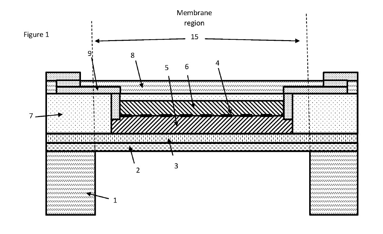
[0048]FIG. 1 shows a cross section of a heterostructure-based infra-red device that can be operated as IR emitter and / or as IR detector;

[0049]FIG. 2 shows a top view of a heterostructure-based infra-red device that can be operated as IR emitter and / or as IR detector;

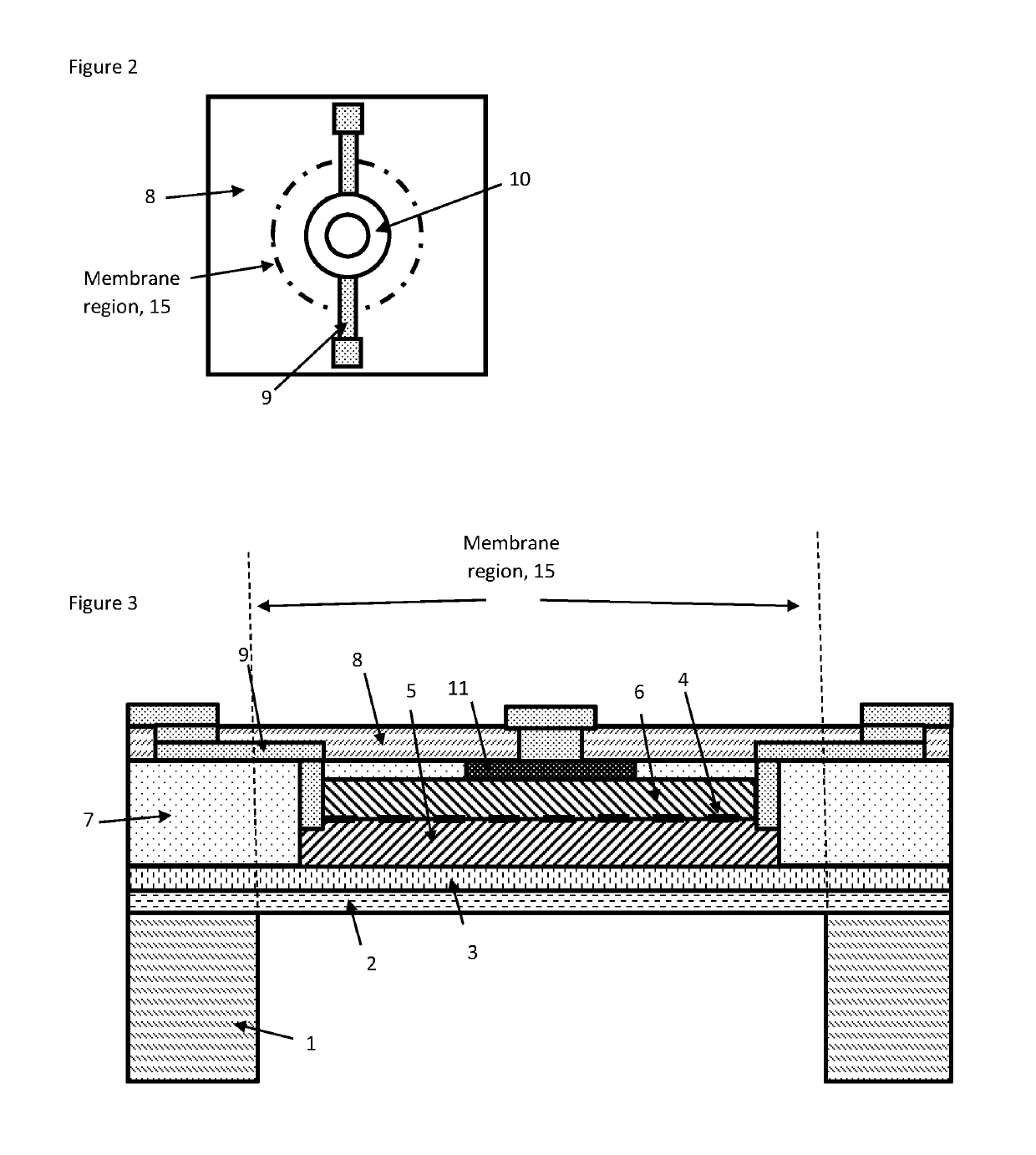
[0050]FIG. 3 shows a cross section of a heterostructure-based infra-red device that can be operated as IR emitter and / or as IR detector. The heating element and / or the temperature sensing element is in form of an HEMT;

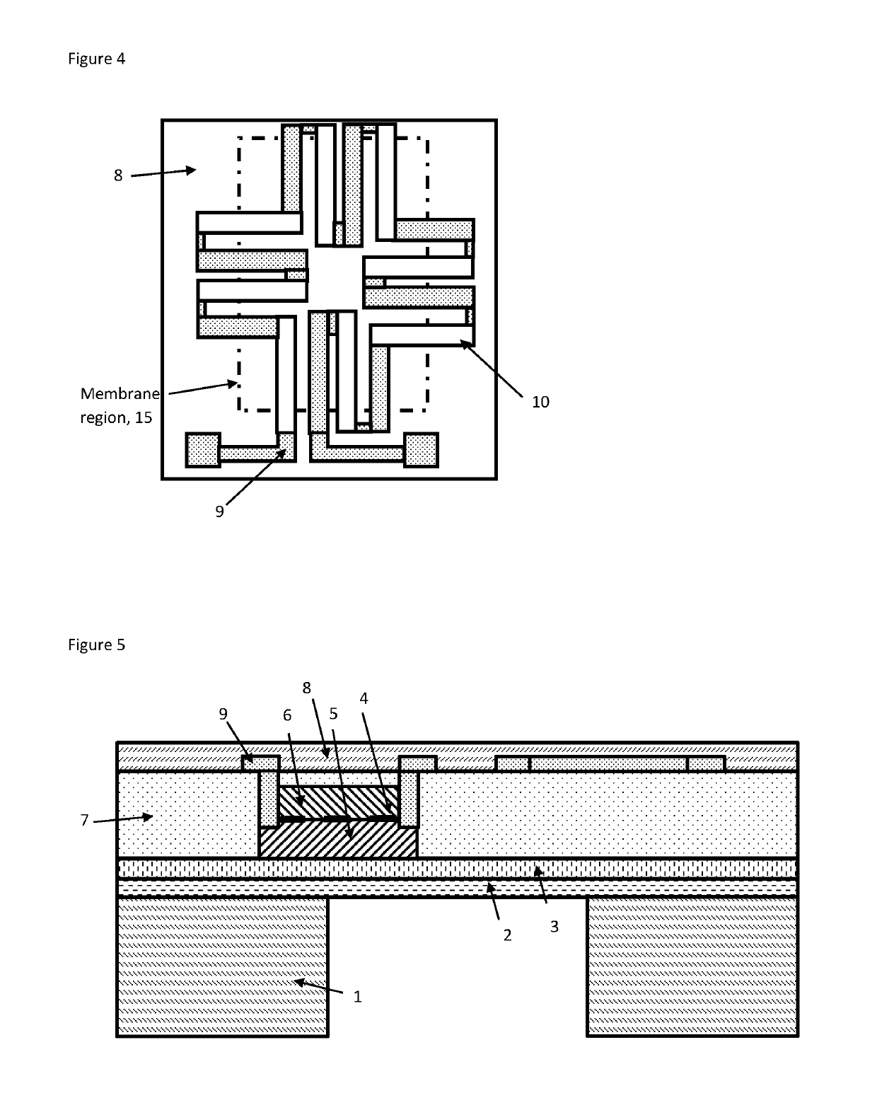
[0051]FIG. 4 shows a top view of a heterostructure-based infra-red device that can be operated as IR detector. The temperature sensing element of the IR detector is in form of a thermopile;

[0052]FIG. 5 shows a cross section of a heterostructure-based infra-red device that can be operated as IR detector. The temperature sensing element of the IR detector is...


PUM


Abstract

We disclose herewith a heterostructure-based infra-red (IR) device comprising a substrate comprising an etched portion and a substrate portion; a device region on the etched portion and the substrate portion, the device region comprising a membrane region which is an area over the etched portion of the substrate. At least one heterostructure-based element is formed at least partially within or on the membrane region and the heterostructure-based element comprises at least one two dimensional carrier gas.

Description

TECHNICAL FIELD[0001]This disclosure relates to micro-machined thermal infra-red (IR) devices. Particularly but not exclusively the disclosure relates to heterostructure-based IR emitters and IR detectors with tailored and electrically tunable optical properties.BACKGROUND OF THE DISCLOSURE[0002]It is well known how to fabricate thermal IR emitters. Such devices typically consist of a resistive micro-heater embedded within a thin membrane and supported on a substrate. When current is passed through the heater, it heats up to a high temperature (which can be as much as 700° C. or even higher), and at this high temperature the device emits IR radiation.[0003]A large number of designs with IR emitters have been reported. For example, Parameswaran et al. “Micro-machined thermal emitter from a commercial CMOS process,” IEEE EDL 1991 reports a polysilicon heater for IR applications made in CMOS technology, with a front side etch to suspend the heater and hence reduce power consumption. Si...

Claims


Application Information

Patent Timeline
IPC IPC(8): H01L33/00H01L33/32H01L31/0304H01L35/30H01L27/15H01L31/109H01L31/112H01L27/144H01L35/34H01L31/18H01L27/16H01L35/22H05B3/28
CPCH01L35/34H01L33/0025H01L33/32H01L33/0041H01L33/0075H01L31/03048H01L31/112H01L27/15H01L31/1856H01L27/16H05B3/28H01L31/1848H01L31/109H01L35/22H01L27/1446H01L27/1443H01L31/03044H01L35/30H05B2203/032H05B2203/017H05B3/141H05B3/265H10N19/00H10N10/855H10N10/01H10N10/13G01F1/6845G01F1/688G01F1/69G01F1/7084G01P5/12G01P5/18G01P13/006H01L31/035281G01K7/015H01K1/04H01K1/14H01L33/06H10N10/17
Inventor UDREA, FLORINDE LUCA, ANDREALONGOBARDI, GIORGIA
Owner CAMBRIDGE GAN DEVICES LIMITED
Why Eureka
Try Eureka