Low noise amplifier with improved absolute maximum rating performance
a technology of absolute maximum rating which is applied in the direction low frequency amplifier, amplifier with diodes, etc., can solve the problems of affecting the stability and durability affecting the transmission of rf signals, and heavy burden on internal components (such as transistors) of low noise amplifier, so as to improve the absolute maximum rating performance, improve the stability and durability of transistor and low noise amplifier, and increase the input power
- Summary
- Abstract
- Description
- Claims
- Application Information
AI Technical Summary
Benefits of technology
Problems solved by technology
Method used
Image
Examples
first embodiment
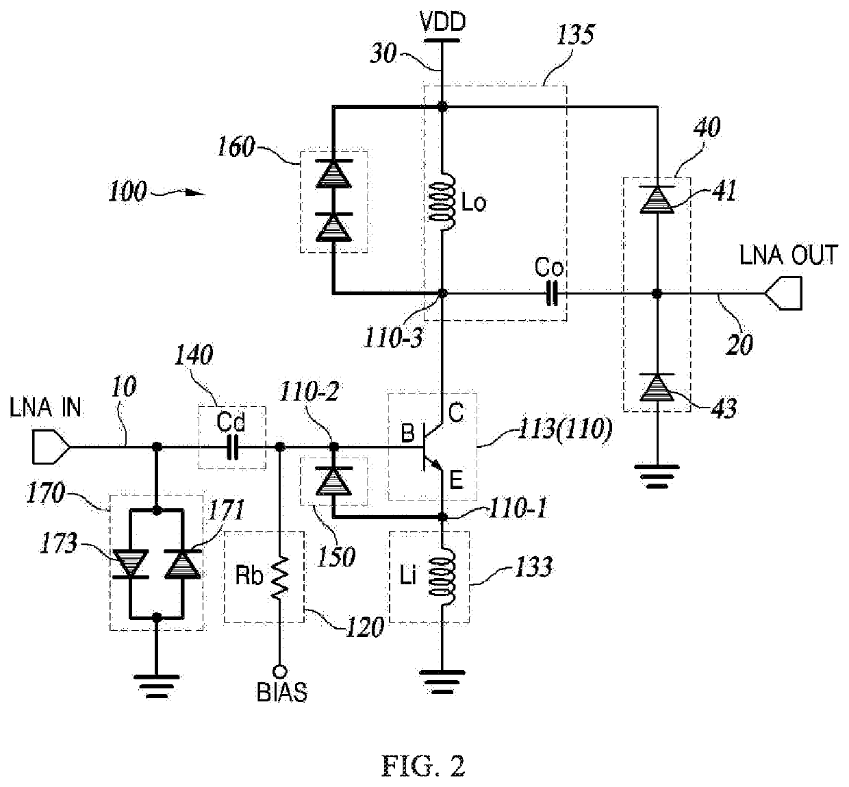
[0032]FIG. 2 illustrates the low noise amplifier 100 of the present disclosure which uses diode for adjusting voltages applied to the terminals of the BJT 113. The following description illustrates the low noise amplifier 100 having the BJT 113 of the present disclosure.
[0033]As shown in FIG. 2, the low noise amplifier 100 of the present disclosure includes the BJT 113, a bias unit 120, an impedance matching unit 130, a blocking capacitor 140, and a first diode unit 150.
[0034]As shown in FIG. 2, an input signal is connected to the BJT 113 of the low noise amplifier 100 of the first embodiment through an input line 10. The low noise amplifier 100 amplifies alternating signals inputted though the input line 10 and outputs amplified signals through an outputting line 20. Preferably, the alternating signals are alternating current or alternating voltages.
[0035]The BJT 113 can be a common-emitter (CE) amplifier, a common-base (CB) amplifier, or a common-collector (CC) amplifier. The BJT ...
third embodiment
[0068]FIG. 2 illustrates an example in which the third diode unit 170 of the present disclosure is constructed of two back-to-back diodes. Based on the back-to-back structure shown in FIG. 2, the present disclosure restricts the inputting under the third standard voltage.
[0069]In the back-to-back diodes, if applying an input signal having a voltage higher than +1 V, the diode 173 (the left diode) on the left side is biased in the forward direction, and the diode 171 (the right diode) on the right side is biased in reverse direction.
[0070]Therefore, the current of the input signal is discharged to the ground GND through the left side diode 173 which is forward biased. Thus, the voltage applied to the first diode unit 150 can be prevented from being higher +1 V than a clamping voltage.
[0071]In contrast, if applying an input signal having a voltage lower than −1 V, the left side diode 173 in the back-to-back diodes is reverse biased, and the right side diode 171 is forward biased.
[0072...
PUM
 Abstract
Description
Claims
Application Information


