This helps you quickly interpret patents by identifying the three key elements:
Problems solved by technology
Method used
Benefits of technology
Benefits of technology
The present invention provides an avalanche photodiode that is designed to avoid edge breakdown and noise in a tunnelling mode. It also ensures a uniform distribution of electric field strength, which allows for uniform operation across the entire avalanche junction. This results in improved performance and reliability of the device.
Problems solved by technology
This is because, when the shape is, for example, quadrangle, the depletion layer does not uniformly spread in the corner portions during application of a voltage; as a result, the electric field strength becomes high locally, to cause breakdown first in the corner portions.
This is because high junction concentration causes steeper band curves between the P-type diffusion layer and the N-type diffusion layer forming the junction, which causes generation of a noise component of band-to-band tunneling mode, resulting in an increase in the dark count noise.
In the case in FIG. 9, the P-well diffusion layer 1106 is used as the guard ring; however, such a guard ring cannot be used in the structure in FIG. 10, so that another structure is required to address edge breakdown.
Method used
Image
Click on the blue label to locate the original text in one second.
Reading with bidirectional positioning of images and text.
Examples
first embodiment
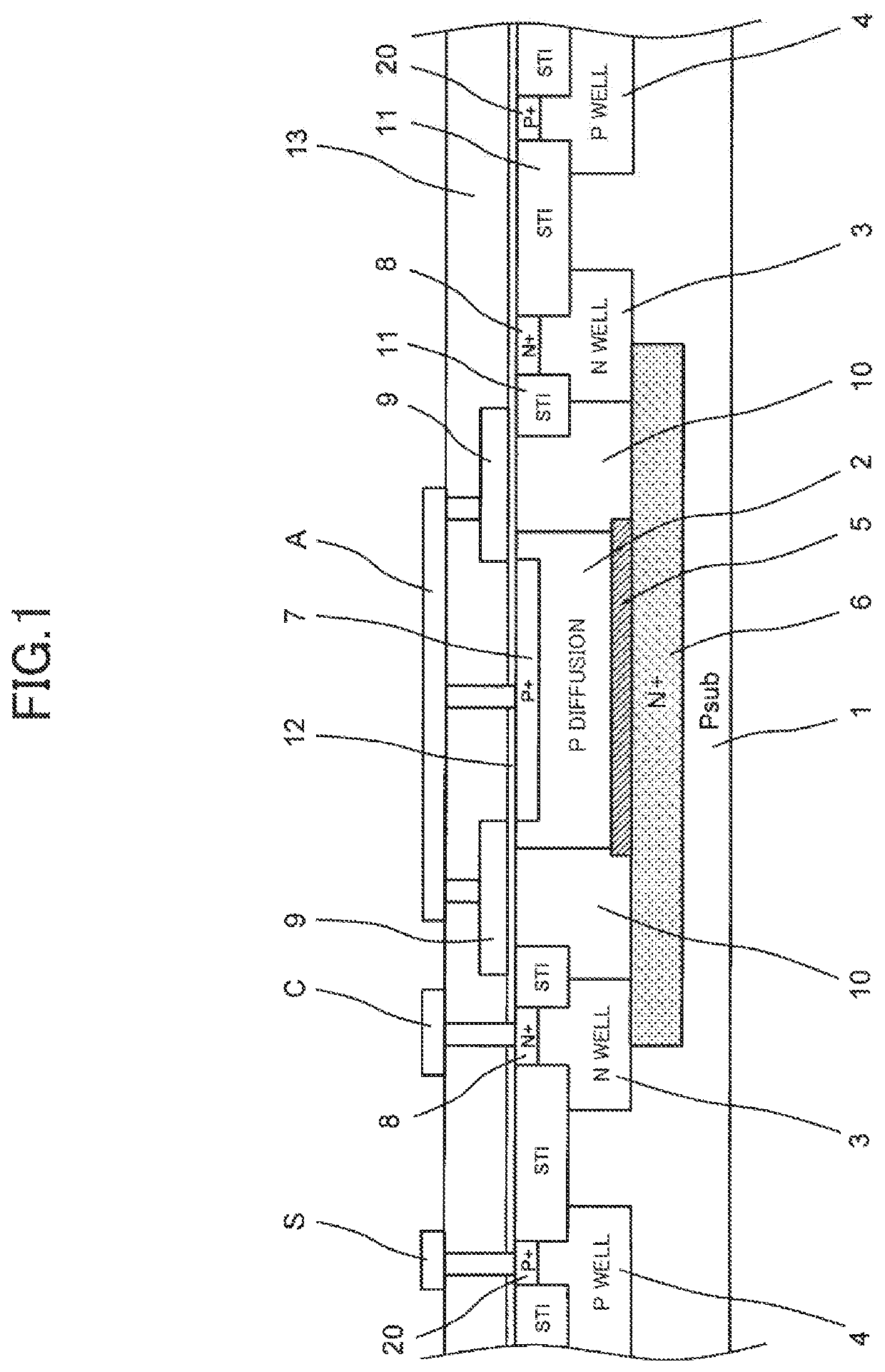
[0050]An avalanche photodiode according to the first embodiment of the present invention will be specifically described with reference to FIG. 1.
[0051]FIG. 1 is a sectional view of the avalanche photodiode according to the first embodiment of the present invention. In this avalanche photodiode, within a silicon semiconductor substrate 1, which, for example, has a plane orientation of (100) and a resistivity of about 10 Ωcm and is of P type, a low-concentration P-type diffusion layer 2 is formed, which serves as a P-type diffusion layer of an avalanche junction. This low-concentration P-type diffusion layer 2 is formed by ion implantation of boron (11B+). For example, boron (11B+) is implanted under the following three-stage ion implantation conditions.
[0052]Incidentally, the dose is described with floating-point representation in which an exponential base of 10 is represented by symbol E. For exam...
second embodiment
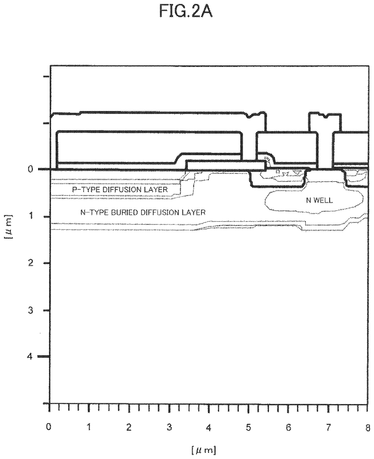
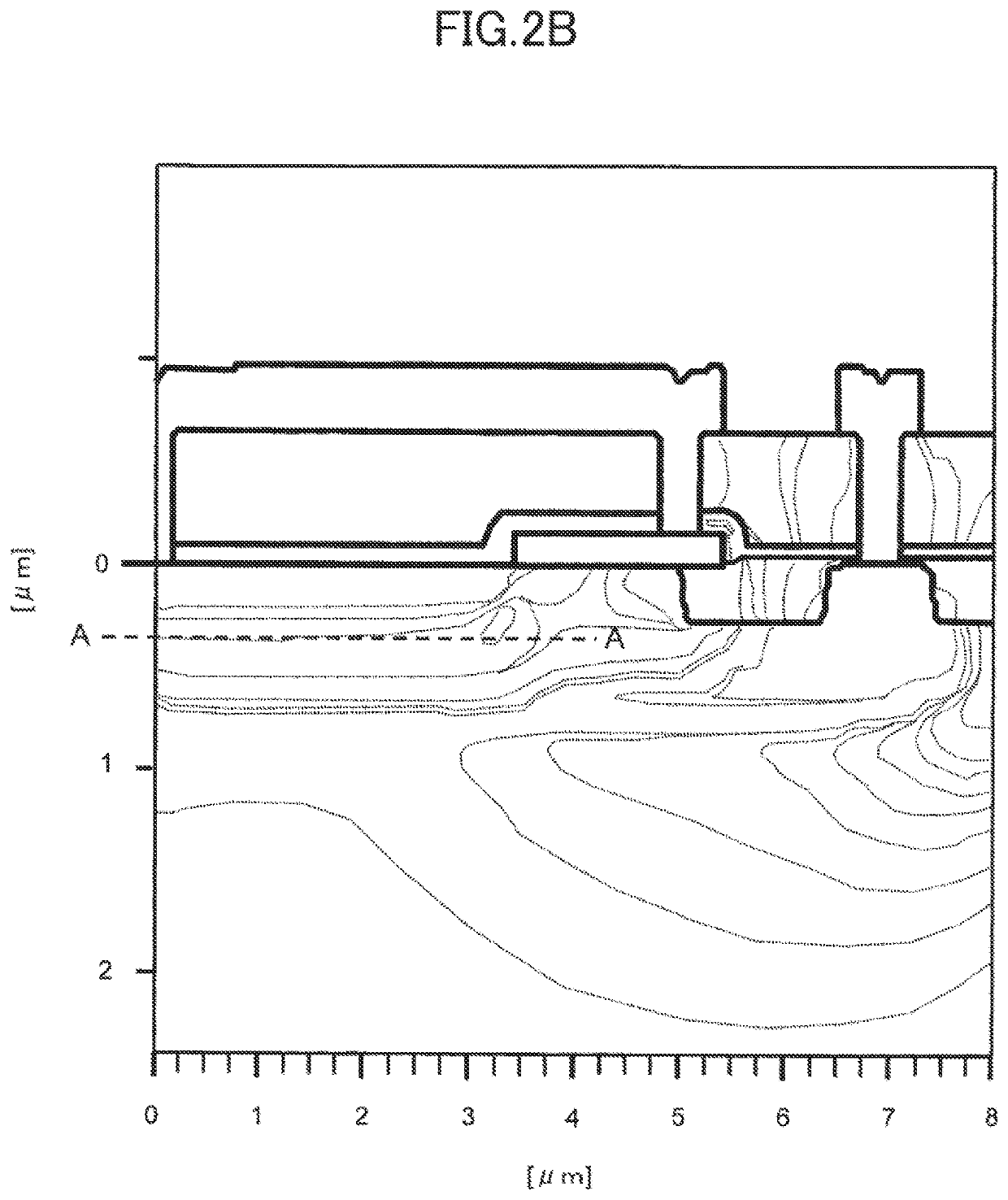
[0078]An avalanche photodiode according to a second embodiment of the present invention will be described with reference to FIG. 4. The basic configuration is the same as in the first embodiment. This avalanche photodiode according to the second embodiment has the same configuration as in the avalanche photodiode according to the first embodiment except for an N-type buried diffusion layer 25.
[0079]In the avalanche photodiode according to the second embodiment, the N-type buried diffusion layer 25 forming the avalanche junction is formed smaller than, in plan view for the substrate, the bottom portion of the low-concentration P-type diffusion layer 2.
[0080]As in the first embodiment, even when the N-type buried diffusion layer 5 forming the avalanche junction is formed larger than the low-concentration P-type diffusion layer 2, as long as it is substantially not connected to the N-type diffusion layer 3, the potential does not automatically become high, so that the above-described a...
third embodiment
[0083]An avalanche photodiode according to a third embodiment of the present invention will be described with reference to FIG. 5. The basic configuration is the same as in the first embodiment. The difference from the avalanche photodiode according to the first embodiment is another high-concentration N-type buried diffusion layer 35 formed between the N-type diffusion layer 3 serving as the cathode diffusion layer and the N-type buried diffusion layer 6. This N-type buried diffusion layer 35 is an example of the fourth second-conductivity-type semiconductor layer.
[0084]As described in the end of the first embodiment, when the N-type buried diffusion layer 6 is formed at a high ion implantation energy and, as a result, formed at a deep position, the contact concentration between the N-type diffusion layer 3 and the N-type buried diffusion layer 6 becomes low, and the isolation strength between the low-concentration P-type diffusion layer 2 and the P-type semiconductor substrate 1 b...
PUM
Abstract
An avalanche photodiode includes a first-conductivity-type semiconductor layer formed within a first-conductivity-type semiconductor substrate; a first second-conductivity-type semiconductor layer formed so as to surround, in plan view for the substrate, with a gap width, the first-conductivity-type semiconductor layer; a second second-conductivity-type semiconductor layer formed deeper than the first-conductivity-type semiconductor layer and in contact with the bottom portion of the first-conductivity-type semiconductor layer; and a third second-conductivity-type semiconductor layer formed deeper than the second second-conductivity-type semiconductor layer and in contact with the bottom portion of the second second-conductivity-type semiconductor layer; anda fourth second-conductivity-type semiconductor layer formed between the first second-conductivity-type semiconductor layer and the third second-conductivity-type semiconductor layer so as to be in contact with at least a portion of a bottom portion of the first second-conductivity-type semiconductor layer; and a fifth second-conductivity-type semiconductor layer formed in an upper portion of the first second-conductivity-type semiconductor layer and having a higher impurity concentration than the first second-conductivity-type semiconductor layer.The first-conductivity-type semiconductor layer and the second second-conductivity-type semiconductor layer form an avalanche junction. The first and third second-conductivity-type semiconductor layers are electrically connected together via the fourth second-conductivity-type semiconductor layer such that the semiconductor substrate and the first-conductivity-type semiconductor layer are electrically isolated from each other.
Description
CROSS REFERENCES TO RELATED APPLICATIONS[0001]This application claims the benefit of priority to Japanese Patent Application No. 2016-192074, filed Sep. 29, 2016, and the entire contents of which are herein incorporated by reference.TECHNICAL FIELD[0002]The present invention relates to an avalanche photodiode, specifically to an avalanche photodiode that has a structure configured to prevent edge breakdown and have a uniform electric-field distribution.BACKGROUND ART[0003]In these years, range-finding sensors have been used for autofocus of cellular phone cameras and for determination of position or distance for automatic robots such as robotic cleaners. In particular, photosensors such as TOF (Time Of Flight) sensors employing avalanche photodiodes operating in Geiger mode have been used because these sensors can determine distance in dark fields and can be provided in reduced sizes.[0004]Avalanche photodiodes are one type of PN diodes used so as to cause avalanche breakdown. In th...
Claims
Application Information
Patent Timeline
Application Date:The date an application was filed.
Publication Date:The date a patent or application was officially published.
First Publication Date:The earliest publication date of a patent with the same application number.
Issue Date:Publication date of the patent grant document.
PCT Entry Date:The Entry date of PCT National Phase.
Estimated Expiry Date:The statutory expiry date of a patent right according to the Patent Law, and it is the longest term of protection that the patent right can achieve without the termination of the patent right due to other reasons(Term extension factor has been taken into account ).
Invalid Date:Actual expiry date is based on effective date or publication date of legal transaction data of invalid patent.

