Facet region detecting method and detecting apparatus

Active Publication Date: 2020-02-27
DISCO CORP
View PDF4 Cites 2 Cited by
  • Summary
  • Abstract
  • Description
  • Claims
  • Application Information

AI Technical Summary

Benefits of technology

The present invention provides a method and apparatus for easily detecting the facet region of an SiC single crystal ingot. This helps to improve the quality and efficiency of the detection process.

Problems solved by technology

As a result, the modified layer is not formed at a uniform depth, so that a cutting allowance (kerf loss) of a predetermined size is needed even in the case of using a slicing method by a laser beam.
However, in the case of an SiC single crystal ingot which is thicker than the SiC wafer, it is difficult to distinguish the facet region and the non-facet region from each other by visual inspection.
Therefore, in the case of an SiC single crystal ingot, it is difficult to recognize the positions of the respective regions and to apply the laser beam to the SiC single crystal ingot under processing conditions suitable for the respective regions.

Method used


Image

  • Facet region detecting method and detecting apparatus
  • Facet region detecting method and detecting apparatus
  • Facet region detecting method and detecting apparatus

Examples


Embodiment Construction

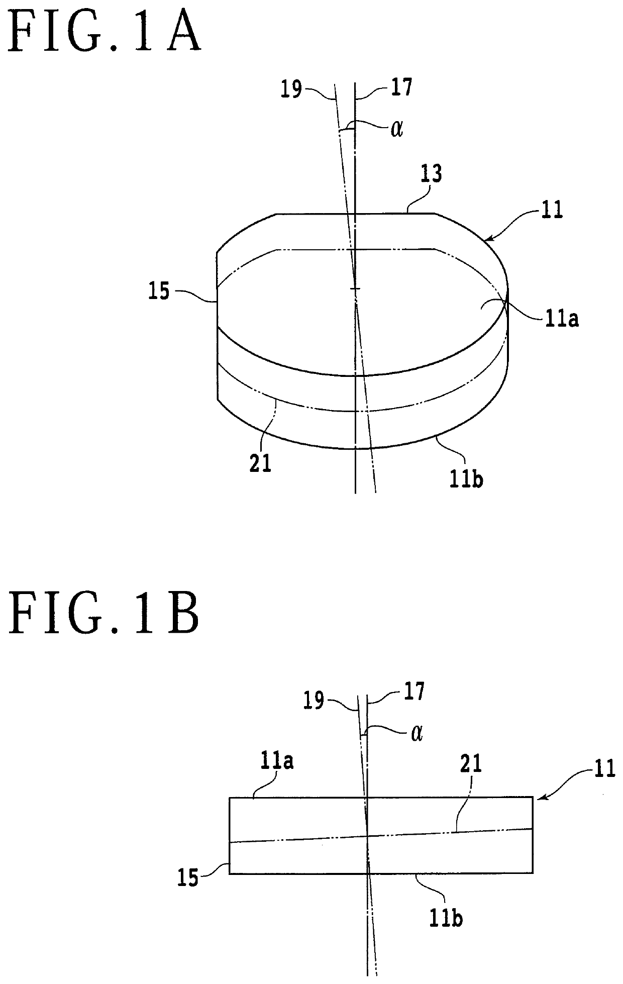
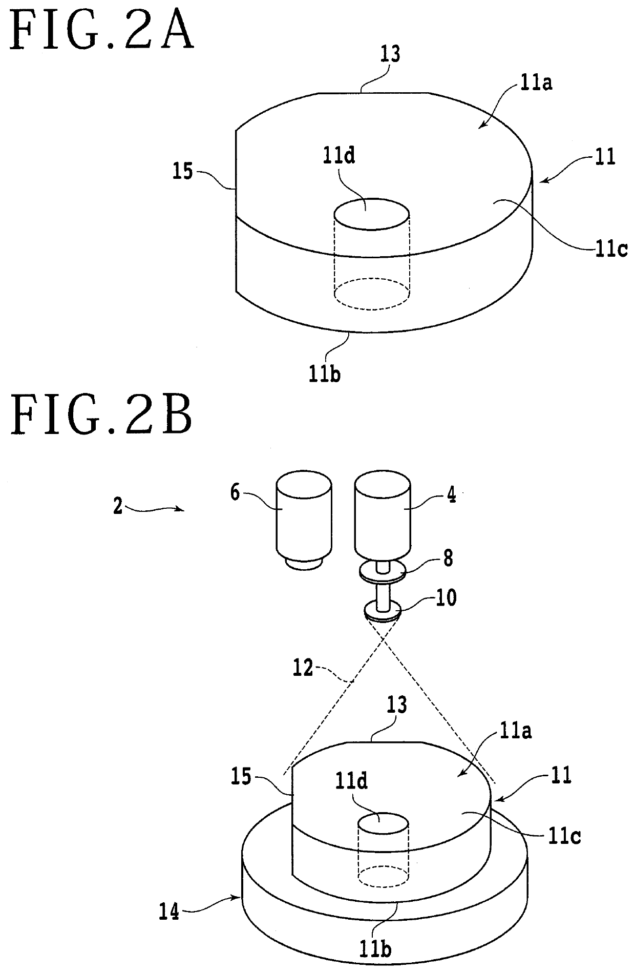
[0024]An embodiment of the present invention will be described below, referring to the attached drawings. First, an SiC single crystal ingot of which a facet region is to be detected by a facet region detecting method and detecting apparatus according to the present embodiment will be described. FIG. 1A is a perspective view schematically depicting an SiC single crystal ingot 11, and FIG. 1B is a side view schematically depicting the SiC single crystal ingot 11. The SiC single crystal ingot 11 has a first surface 11a and a second surface 11bon a side opposite to the first surface 11a. The first surface 11a and the second surface 11b are parallel to each other. The SiC single crystal ingot 11 is, for example, split at a split plane parallel to the first surface 11a, and is sliced as an SiC wafer. The SiC wafer is paid attention as a next-generation semiconductor material to be used for manufacture of power devices such as inverters and converters.

[0025]At the time of splitting the Si...


PUM


Abstract

A facet region detecting method for detecting a facet region of an SiC single crystal ingot includes: an irradiation step of irradiating a first surface of the SiC single crystal ingot with light; a fluorescence intensity detection step of detecting the intensity of fluorescence generated from the first surface of the SiC single crystal ingot by the light; and a determination step of determining a region of the first surface where the fluorescence intensity is comparatively low as a facet region and determining a region where the fluorescence intensity is comparatively high as a non-facet region.

Description

BACKGROUND OF THE INVENTIONField of the Invention[0001]The present invention relates to a detecting method for detecting a facet region of a silicon carbide (SiC) single crystal ingot and a detecting apparatus for detecting the facet region.Description of the Related Art[0002]In recent years, attention has been paid to SiC in place of silicon (Si) as a next-generation semiconductor material to be used for power devices such as inverters and converters. An SiC wafer is formed by slicing an SiC single crystal ingot. As a method for manufacturing an SiC wafer by slicing the SiC single crystal ingot, there has been known, for example, a method in which the SiC single crystal ingot is sliced by use of a wire saw. However, the method using the wire saw has a problem that the amount of SiC lost is large, and the number of SiC wafers obtained is small as compared to the amount of the SiC single crystal ingot serving as a raw material. For example, at the time of manufacturing an SiC wafer w...

Claims


Application Information

Patent Timeline
IPC IPC(8): G01N21/64C30B33/00C30B29/36G01N1/28
CPCG01N1/286C30B29/36C30B33/00G01N21/6489G01N2001/2866G01N21/64H01L22/24G01N21/9501G01N2021/8477H01L22/26C30B35/00H01L22/12H01L22/34H01L21/02013H01L21/02378
Inventor MURAZAWA, NAOKITAKAHASHI, KUNIMITSU
Owner DISCO CORP
Why Eureka
Try Eureka