Flexible substrate with high dielectric-constant film and manufacturing method thereof

Active Publication Date: 2020-06-04
WUHAN CHINA STAR OPTOELECTRONICS SEMICON DISPLAY TECH CO LTD
View PDF5 Cites 0 Cited by
  • Summary
  • Abstract
  • Description
  • Claims
  • Application Information

AI Technical Summary

Benefits of technology

The present invention provides a flexible substrate with a high dielectric-constant film and a manufacturing method thereof, which can effectively reduce a leakage current of a flexible display device, decrease a threshold voltage, improve current regulation, and reduce power consumption. The use of a high dielectric constant material, such as HfAlOx, can provide these benefits and also decrease the thickness of the TFT device, making it suitable for flexible display devices. Moreover, preparing the gate insulating layer with the HfAlOx solution can simplify operations, reduce production costs, and increase production speed. Overall, the invention provides a flexible substrate with improved performance and reduced production costs.

Problems solved by technology

However, as development of flexible display devices, the display device tends to be ultra-thin, and the SiOx / SiNx insulating layer increases a leakage current due to a quantum tunneling effect, resulting in an increase in power consumption of the display device and thereby affecting normal operations of the display device.
In addition, in a conventional process for producing a gate insulating layer, chemical vapor deposition (CVD) or physical vapor deposition (PVD) are used for coating, but these manufacturing methods have high requirements on equipment, and a vacuum environment is required, leading to high production costs and a slow production speed.
As development of flexible display devices, display devices tend to be ultra-thin, and the SiOx / SiNx insulating layer has an increased leakage current due to a quantum tunneling effect, resulting in increased power consumption of the display device and affecting normal operations of the display device.
In addition, in a conventional process for producing a gate insulating layer, chemical vapor deposition (CVD) or physical vapor deposition (PVD) are used for coating, but these manufacturing methods have high requirements on equipment, and a vacuum environment is required, thereby causing high production costs, and a slow production speed.

Method used


Image

  • Flexible substrate with high dielectric-constant film and manufacturing method thereof
  • Flexible substrate with high dielectric-constant film and manufacturing method thereof
  • Flexible substrate with high dielectric-constant film and manufacturing method thereof

Examples


Embodiment Construction

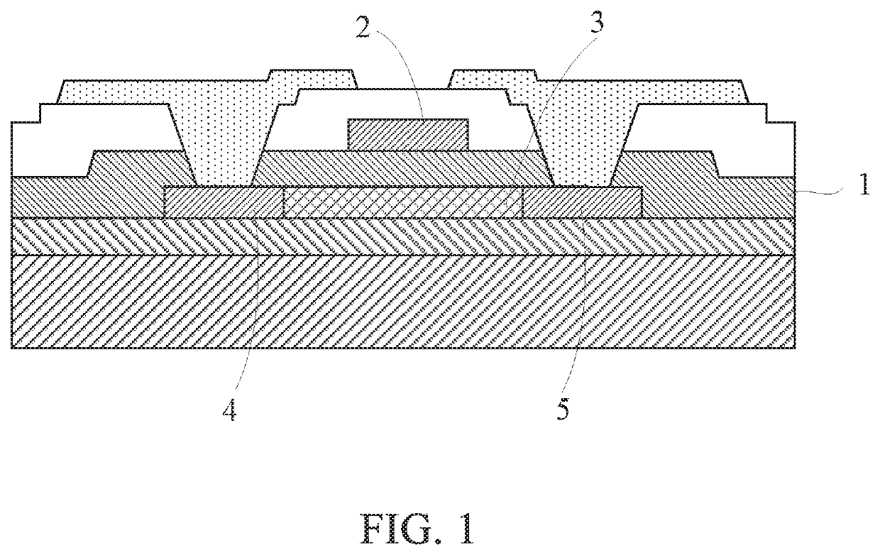
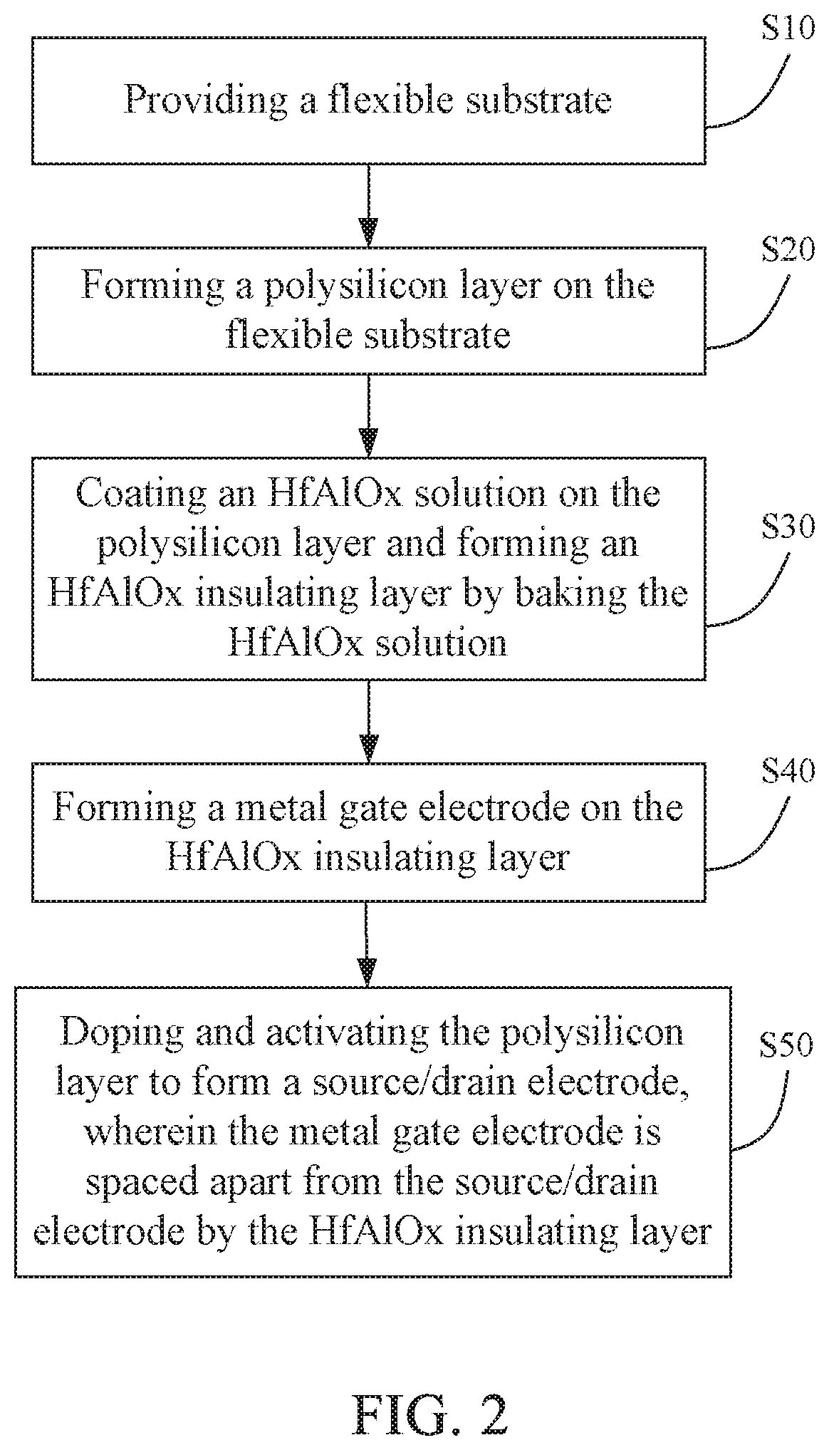
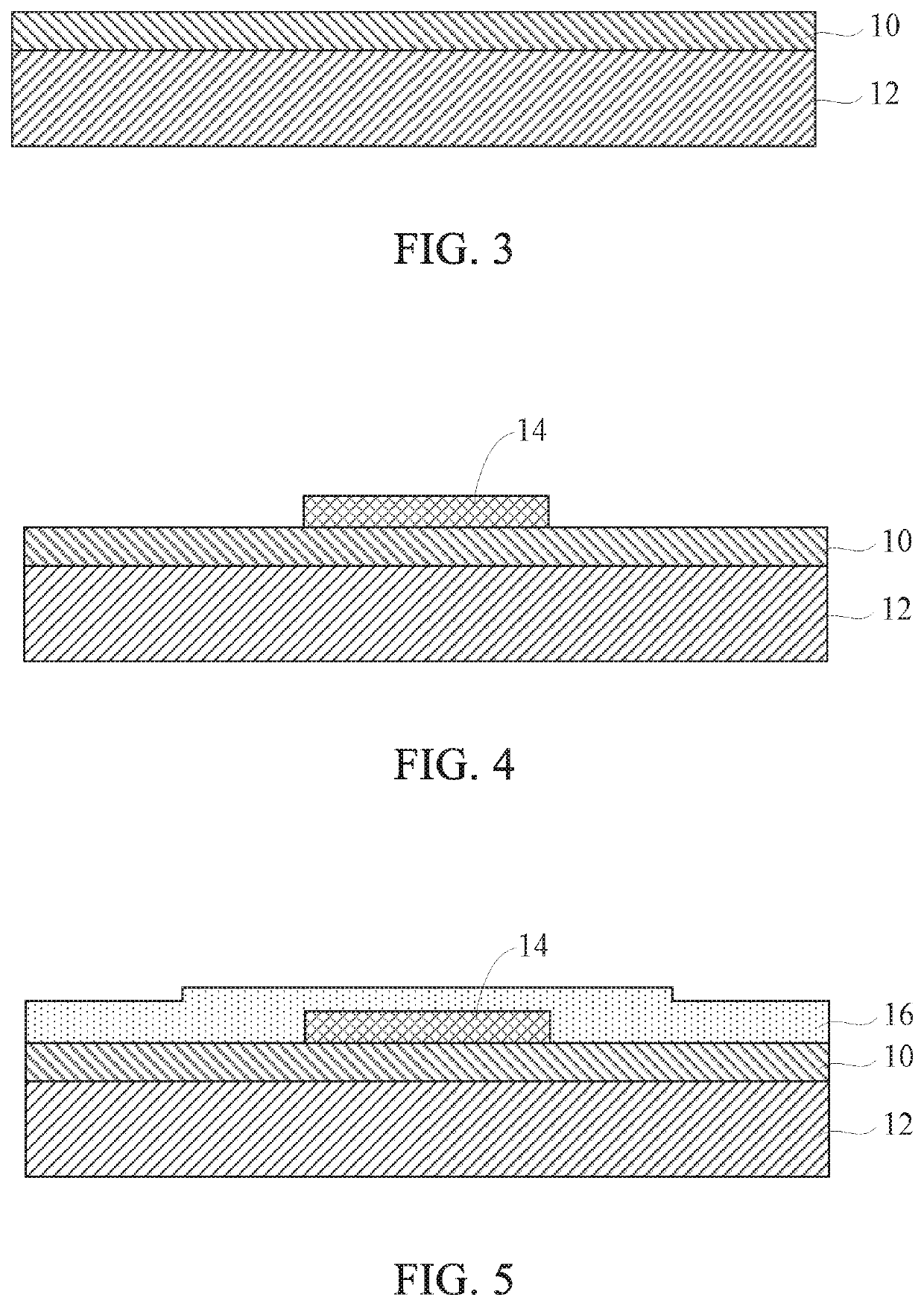
[0043]The word “embodiment” mentioned in the detailed description means that a particular feature, structure, or characteristic described in connection with the embodiment may be included in at least one embodiment of the invention. The same terms appearing in different places in the specification are not necessarily limited to the same embodiment, but can belong to independent or alternative embodiments. In view of the technical solutions disclosed in the embodiments of the present invention, those skilled in the art should understand that the embodiments described herein may have other combinations or variations based on inventive concepts of the technical solutions.

[0044]Embodiments of the present disclosure are described in detail with reference to the accompanying drawings as follows. Directional terms such as up / down, right / left and the like may be used for the purpose of enhancing a reader's understanding about the accompanying drawings, but are not intended to be limiting. S...


PUM


Abstract

The present invention provides a flexible substrate with a high dielectric-constant film and a manufacturing method thereof. The manufacturing method comprises following steps: providing a flexible substrate; forming a polysilicon layer on the flexible substrate; coating an HfAlOx solution on the polysilicon layer and forming an HfAlOx insulating layer by baking or annealing the HfAlOx solution; forming a metal gate electrode on the HfAlOx insulating layer; and doping and activating the polysilicon layer to form a source / drain electrode. The metal gate electrode is spaced apart from the source / drain electrode by the HfAlOx insulating layer.

Description

1. FIELD OF DISCLOSURE[0001]The present invention relates to a field of display devices and, in particular, to a flexible substrate with a high dielectric-constant film and a manufacturing method thereof.2. DESCRIPTION OF RELATED ART[0002]As a core component in flat panel displays, a thin-film transistor (TFT) plays an important role in improving display performance and widening display applications. A threshold voltage, a subthreshold swing, and field-effect mobility of the thin film transistor is directly influenced by electrical properties of a gate insulating layer of a TFT device and by interface properties between the gate insulating layer and a channel of an active layer. As shown in FIG. 1, the gate insulating layer 1 of the TFT device is currently produced by using silicon oxide / silicon nitride (SiOx / SiNx) as an insulating layer to separate the gate electrode 2 from the source electrode 4 and the drain electrode 5 at two sides of the polysilicon layer 3. However, as develop...

Claims


Application Information

Patent Timeline
IPC IPC(8): H01L29/49H01L29/40H01L29/66H01L29/786H01L21/02H01L21/28
CPCH01L21/02194H01L21/02178H01L29/4908H01L29/401H01L29/78603H01L29/78675H01L29/66757H01L21/28158H01L21/02181H01L21/02282
Inventor JIN, PENG
Owner WUHAN CHINA STAR OPTOELECTRONICS SEMICON DISPLAY TECH CO LTD
Why Eureka
Try Eureka