Actinic ray-sensitive or radiation-sensitive resin composition, resist film, pattern forming method, method for manufacturing electronic device

a technology of radiation-sensitive resin and resist film, which is applied in the direction of photosensitive material processing, photomechanical equipment, instruments, etc., can solve the problems of deterioration of collapse suppressing capability, l/s pattern deterioration, and uneven number of photons, and achieve excellent ler and collapse suppressing capability, high sensitivity

Inactive Publication Date: 2020-06-11
FUJIFILM CORP
View PDF1 Cites 1 Cited by
  • Summary
  • Abstract
  • Description
  • Claims
  • Application Information

AI Technical Summary

Benefits of technology

[0040]According to the present invention, it is possible to provide an actinic ray-sensitive or radiation-sensitive resin composition which has high sensitivity and can form a pattern having excellent LER and collapse suppressing capability.
[0041]In addition, according to the present invention, it is possible to provide a resist film, a pattern forming method, and a method for manufacturing an electronic device, each using the actinic ray-sensitive or radiation-sensitive resin composition.

Problems solved by technology

As a result, in lithography with EUV light, an effect of a “photon shot noise” that the number of photons becomes uneven stochastically is significant, which has become a major cause of deterioration in line edge roughness (LER).
In addition, it is effective to increase the film thickness of the resist film to increase the number of absorbed photons, but the aspect ratio of a pattern thus formed is increased, and accordingly, deterioration in collapse suppressing capability is likely to occur in a line / space (L / S) pattern.
On the other hand, they have also confirmed that in a case where many fluorine atoms are included in a resin, collapse suppressing capability of a pattern thus formed is easily deteriorated.

Method used


Image

  • Actinic ray-sensitive or radiation-sensitive resin composition, resist film, pattern forming method, method for manufacturing electronic device
  • Actinic ray-sensitive or radiation-sensitive resin composition, resist film, pattern forming method, method for manufacturing electronic device
  • Actinic ray-sensitive or radiation-sensitive resin composition, resist film, pattern forming method, method for manufacturing electronic device

Examples


examples

[0402]Hereinbelow, the present invention will be described in more detail with reference to Examples. The materials, the amounts of materials used, the proportions, the treatment details, the treatment procedure, and the like shown in the Examples below may be modified as appropriate as long as the modifications do not depart from the spirit of the present invention. Therefore, the scope of the present invention should not be construed as being limited to the Examples set forth below.

[0403][Resin]

[0404]The respective repeating units in resins P-1 to P-29 shown in Table 1 are set forth below.

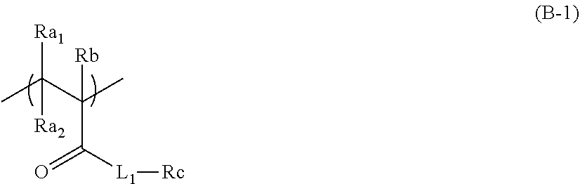
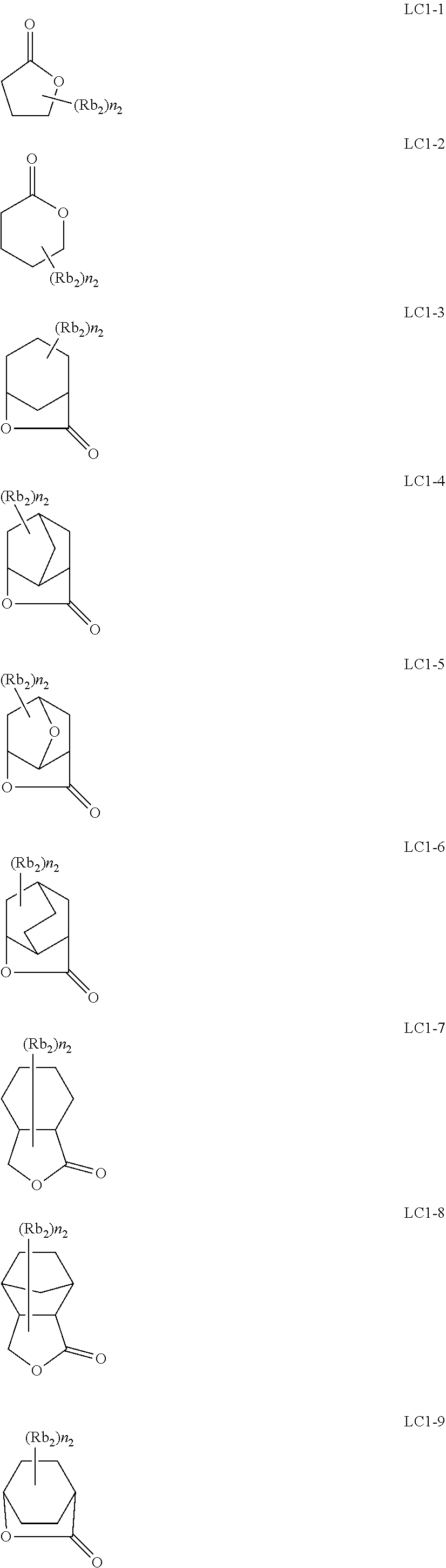
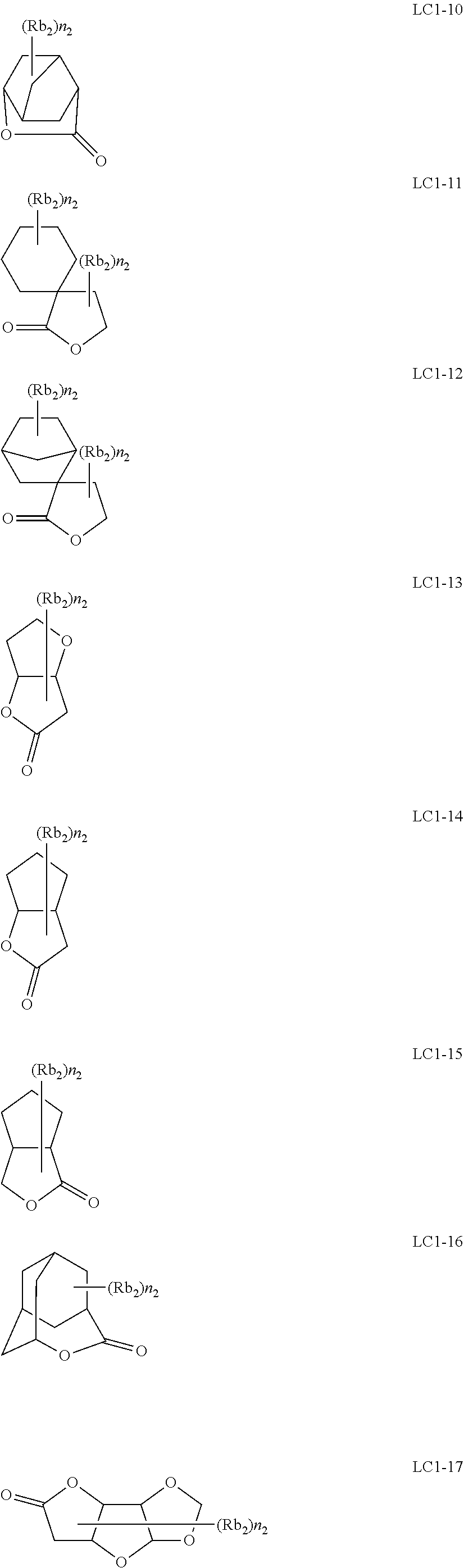
[0405]Moreover, in the respective repeating units set forth below, MA-3, MB-3, MB-4, MC-1, MC-3, MC-6, MC-7, and MC-8 each correspond to a repeating unit represented by General Formula (B-2).

[0406]Furthermore, MC-3 corresponds to a repeating unit (A), MB-3 and MB-4 each correspond to a repeating unit (B), and MA-3 corresponds to the above-mentioned repeating unit (C).

[0407]In addition, MA-3, MB-3...


PUM

PropertyMeasurementUnit
wavelengthaaaaaaaaaa
pKaaaaaaaaaaa

Abstract

An actinic ray-sensitive or radiation-sensitive resin composition is an actinic ray-sensitive or radiation-sensitive resin composition including a compound that generates an acid upon irradiation with actinic rays or radiation and a resin capable of increasing polarity by the action of an acid, in which the resin includes a repeating unit represented by General Formula (B-1) and at least one halogen atom selected from the group consisting of a fluorine atom and an iodine atom.

Description

CROSS-REFERENCE TO RELATED APPLICATIONS[0001]This application is a Continuation of PCT International Application No. PCT / JP2018 / 026910 filed on Jul. 18, 2018, which claims priority under 35 U.S.C § 119(a) to Japanese Patent Application No. 2017-167780 filed on Aug. 31, 2017. Each of the above application(s) is hereby expressly incorporated by reference, in its entirety, into the present application.BACKGROUND OF THE INVENTION1. Field of the Invention[0002]The present invention relates to an actinic ray-sensitive or radiation-sensitive resin composition, a resist film, a pattern forming method, and a method for manufacturing an electronic device.2. DESCRIPTION OF THE RELATED ART[0003]In processes for manufacturing semiconductor devices such as an integrated circuit (IC) and a large scale integrated circuit (LSI) in the related art, microfabrication by lithography using a photoresist composition (hereinafter also referred to as an “actinic ray-sensitive or radiation-sensitive resin co...

Claims


Application Information

Patent Timeline
Patent Type & Authority Applications(United States)
IPC IPC(8): G03F7/039G03F7/004G03F7/038C08L33/06C08L33/16
CPCC08L33/16G03F7/0392G03F7/0045C08L33/066G03F7/0382C08F20/22G03F7/0046G03F7/0397C08F212/24C08F220/24C08F212/20C08F212/22C09D125/18C08F220/1806C08F212/08C08F212/14G03F7/004G03F7/039G03F7/20G03F7/26
Inventor OGAWA, MICHIHIROKANEKO, AKIHIROKAWASHIMA, TAKASHITSUCHIMURA, TOMOTAKA
Owner FUJIFILM CORP
Why Eureka
Try Eureka