Electrical overstress protection with low leakage current for high voltage tolerant high speed interfaces

a high-speed interface and low-leakage current technology, applied in the field of low-leakage, low capacitance, and/or high-voltage-tolerant electrical overstress protection, can solve the problems of increasing ic temperature, electrical overstress events in certain electronic systems, damage or destroy integrated circuits, etc., and achieves low leakage current, low capacitance, and reduced leakage current at the pad

Active Publication Date: 2020-07-16
ANALOG DEVICES INT UNLTD
View PDF0 Cites 8 Cited by
  • Summary
  • Abstract
  • Description
  • Claims
  • Application Information

AI Technical Summary

Benefits of technology

[0005]Electrical overstress protection with low leakage current and low capacitance is provided. In certain embodiments, a semiconductor chip includes a power clamp for protecting against electrical overstress at a pad of the chip's electrical interface. The power clamp is isolated from the pad by at least one isolation blocking voltage device. By interposing the isolation blocking voltage device between the pad and the power clamp, the pad is shielded from a capacitance of the power clamp and / or an amount of leakage current at the pad is reduced. Thus, the electrical interface can operate with high speed, rapid signaling, and / or low static power dissipation while maintaining robustness in the presence of electrical overstress that could otherwise damage the semiconductor chip.

Problems solved by technology

Certain electronic systems can be exposed to electrical overstress events, or electrical signals of short duration having rapidly changing voltage and high power.
Electrical overstress events can damage or destroy integrated circuits (ICs) by generating overvoltage conditions and high levels of power dissipation in relatively small areas of the ICs.
High power dissipation can increase IC temperature, and can lead to numerous problems, such as gate oxide punch-through, junction damage, metal damage, and surface charge accumulation.

Method used


Image

  • Electrical overstress protection with low leakage current for high voltage tolerant high speed interfaces
  • Electrical overstress protection with low leakage current for high voltage tolerant high speed interfaces
  • Electrical overstress protection with low leakage current for high voltage tolerant high speed interfaces

Examples


Embodiment Construction

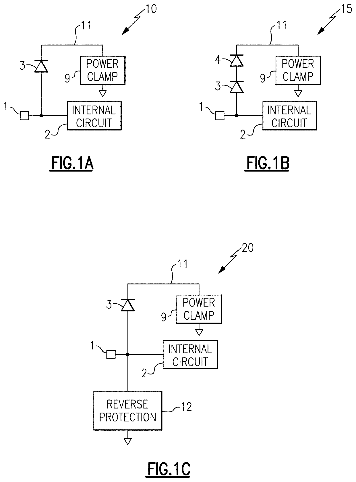
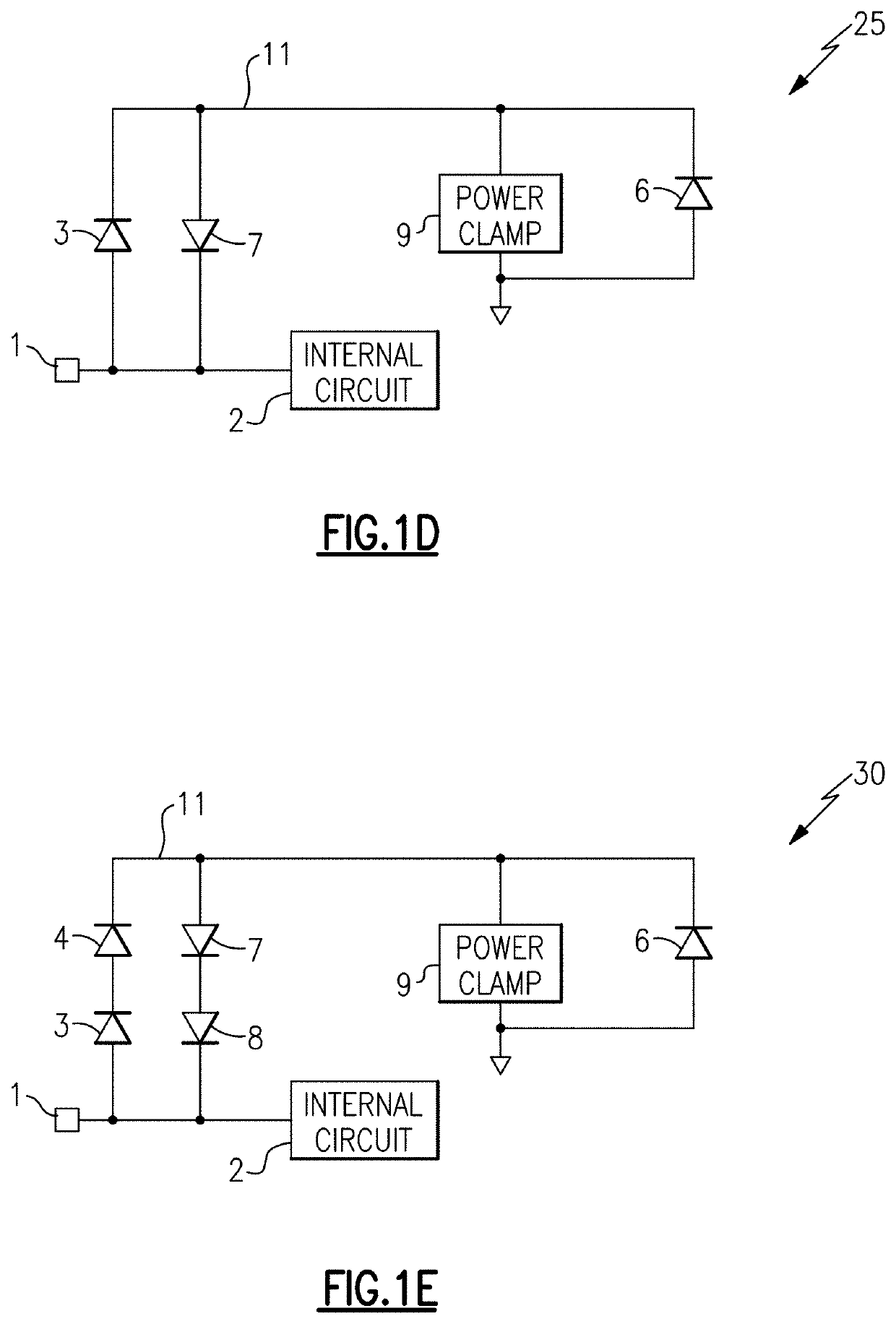
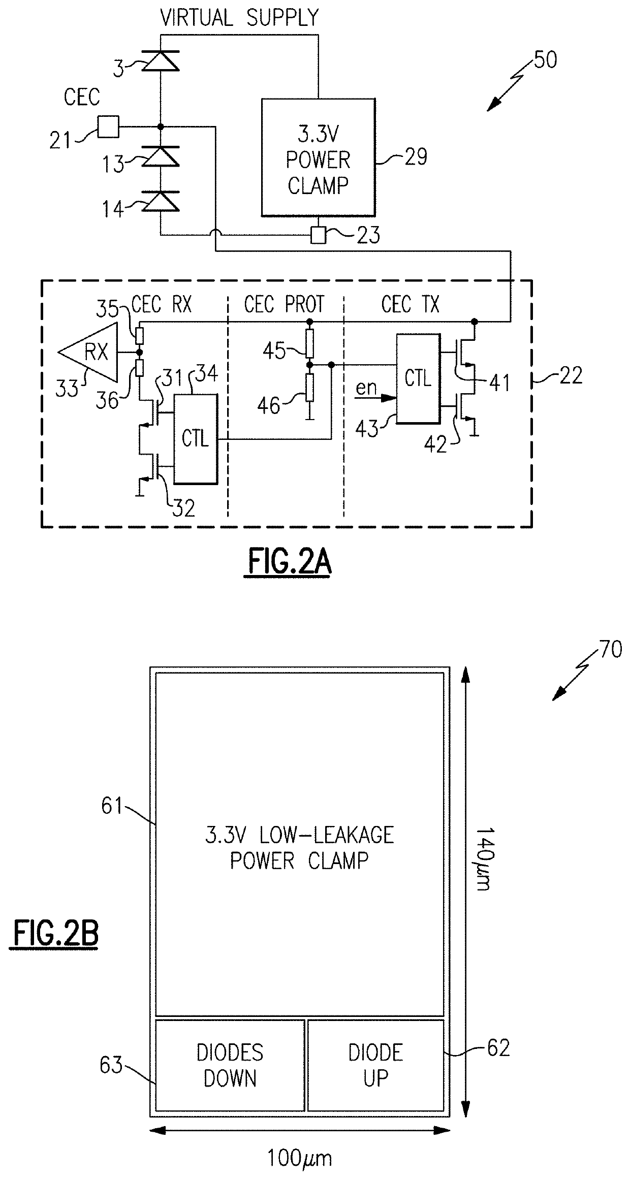
[0048]The following detailed description of embodiments presents various descriptions of specific embodiments of the invention. However, the invention can be embodied in a multitude of different ways. In this description, reference is made to the drawings where like reference numerals may indicate identical or functionally similar elements. It will be understood that elements illustrated in the figures are not necessarily drawn to scale. Moreover, it will be understood that certain embodiments can include more elements than illustrated in a drawing and / or a subset of the elements illustrated in a drawing. Further, some embodiments can incorporate any suitable combination of features from two or more drawings.

[0049]Certain electronic systems include overstress protection circuits to protect circuits or components from electrical overstress events. To help guarantee that an electronic system is reliable, manufacturers can test the electronic system under defined stress conditions, whi...


PUM

PropertyMeasurementUnit
trigger voltageaaaaaaaaaa
widthaaaaaaaaaa
widthaaaaaaaaaa

Abstract

High voltage tolerant electrical overstress protection with low leakage current and low capacitance is provided. In one embodiment, a semiconductor die includes a signal pad, an internal circuit electrically connected to the signal pad, a power clamp electrically connected to an isolated node, and one or more isolation blocking voltage devices electrically connected between the signal pad and the isolated node. The one or more isolation blocking voltage devices are operable to isolate the signal pad from a capacitance of the power clamp. In another embodiment, a semiconductor die includes a signal pad, a ground pad, a high voltage/high speed internal circuit electrically connected to the signal pad, and a first thyristor and a second thyristor between the signal pad and the ground pad.

Description

CROSS-REFERENCE TO RELATED APPLICATIONS[0001]The present application claims priority to U.S. Provisional Patent Application No. 62 / 790,822, filed Jan. 10, 2019, and titled “ELECTRICAL OVERSTRESS PROTECTION WITH LOW LEAKAGE CURRENT AND LOW CAPACITANCE,” the entirety of which is hereby incorporated herein by reference.FIELD OF THE DISCLOSURE[0002]Embodiments of the invention relate to electronic systems, and more particularly to low leakage, low capacitance, and / or high voltage tolerant electrical overstress protection.BACKGROUND[0003]Certain electronic systems can be exposed to electrical overstress events, or electrical signals of short duration having rapidly changing voltage and high power. Electrical overstress events include, for example, electrical overstress (EOS) and electrostatic discharge (ESD) arising from the abrupt release of charge from an object or person to an electronic system.[0004]Electrical overstress events can damage or destroy integrated circuits (ICs) by gener...

Claims


Application Information

Patent Timeline
Patent Type & Authority Applications(United States)
IPC IPC(8): H02H9/04H01L29/739H01L29/08H01L27/02H02H11/00
CPCH01L27/0255H01L27/0262H02H9/046H01L29/0839H02H11/002H01L29/7391H01L29/0834H01L27/0266H01L29/7436H01L29/083
Inventor SALCEDO, JAVIER A.PARTHASARATHY, SRIVATSANBOSCH, ENRIQUE C.
Owner ANALOG DEVICES INT UNLTD
Why Eureka
Try Eureka