
Multilayer ceramic substrate and probe card including same

a multi-layer ceramic substrate and probe card technology, applied in the direction of dielectric characteristics, fixed capacitor details, instruments, etc., can solve the problems of reduced inspection accuracy, multi-layer ceramic substrate, and wiring made of tungsten having a lower electrical conductivity, and achieve high electrical conductivity and low thermal expansion coefficient

Active Publication Date: 2020-08-06
POINT ENG
View PDF0 Cites 1 Cited by
  • Summary
  • Abstract
  • Description
  • Claims
  • Application Information

AI Technical Summary

Benefits of technology

The present invention provides a multilayer ceramic substrate that has a low thermal expansion coefficient and a high electrical conductivity. It is possible to securely fix the multilayer insulation portion, since the insulation portion of an anodic oxide film with pores is provided, allowing the solder to penetrate the pores and harden.

Problems solved by technology

However, the multilayer ceramic substrate has a disadvantage in that the wiring is made of tungsten having a lower electrical conductivity than metals such as copper and gold to withstand the ceramic sintering temperature.
Accordingly, there are problems that thermal deformation may occur in the polyimide resin layer and thus the accuracy of inspection is decreased.

Method used


Image

  • Multilayer ceramic substrate and probe card including same
  • Multilayer ceramic substrate and probe card including same
  • Multilayer ceramic substrate and probe card including same

Examples


Embodiment Construction

[0027]The following merely illustrates the principles of the invention. Therefore, those skilled in the art can implement the principles of the invention and invent various devices included in the concept and scope of the invention, although not explicitly described or illustrated herein. In addition, all conditional terms and embodiments listed herein are in principle clearly intended for the purpose of understanding the concept of the invention and should be understood not to be limited to the specifically listed embodiments and states.

[0028]The above objects, features, and advantages will become more apparent from the following detailed description taken in conjunction with the accompanying drawings, whereby the technical spirit of the invention may be easily implemented by those skilled in the art.

[0029]Hereinafter, preferred embodiments of the present invention will be described in detail with reference to the accompanying drawings.

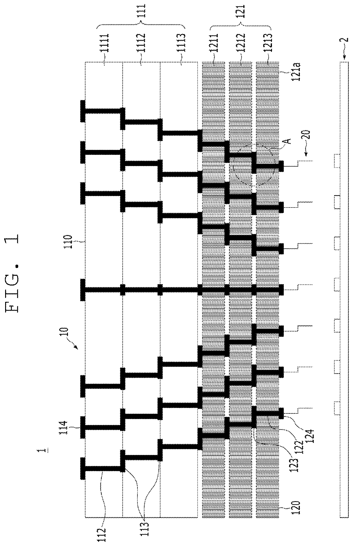
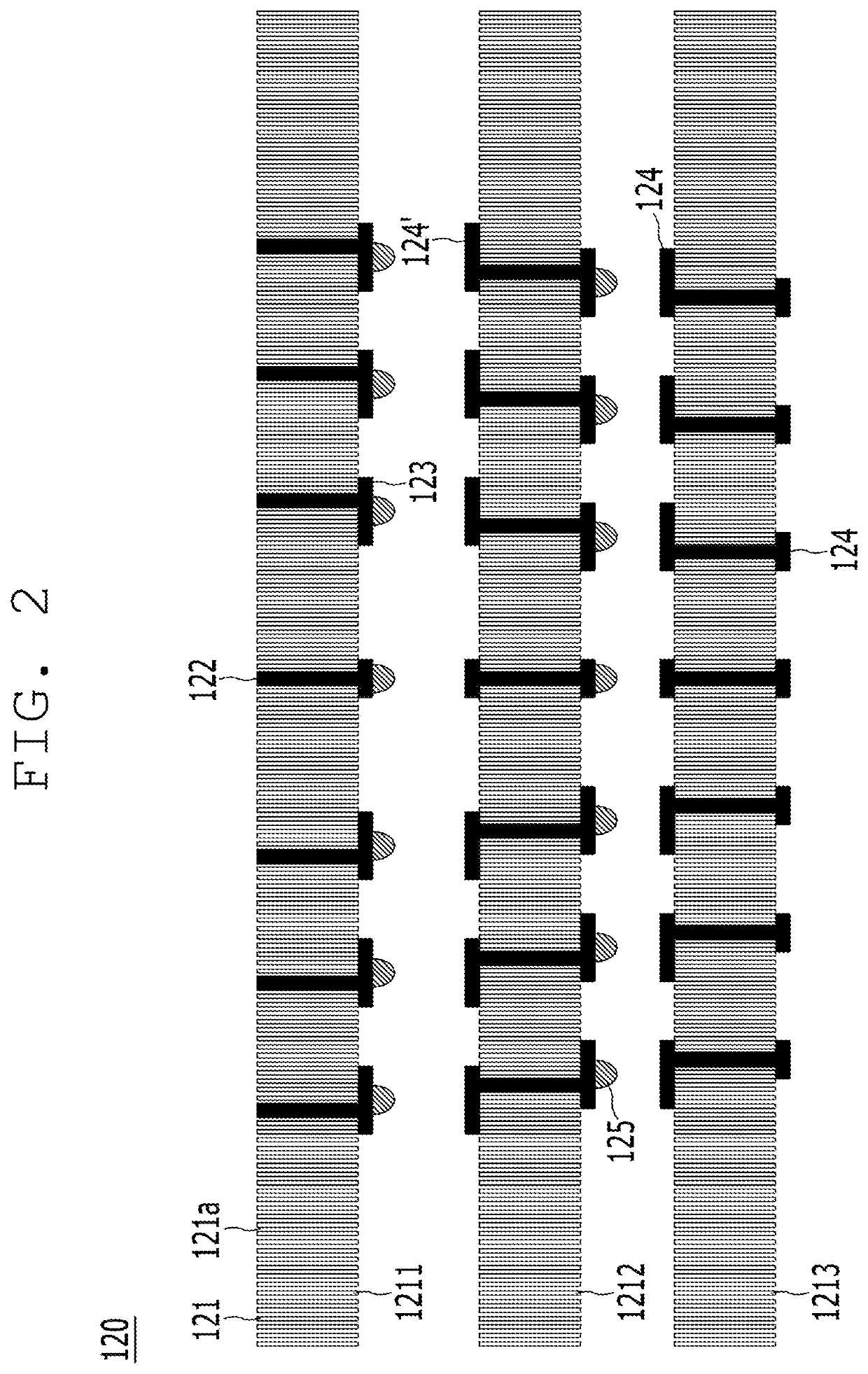
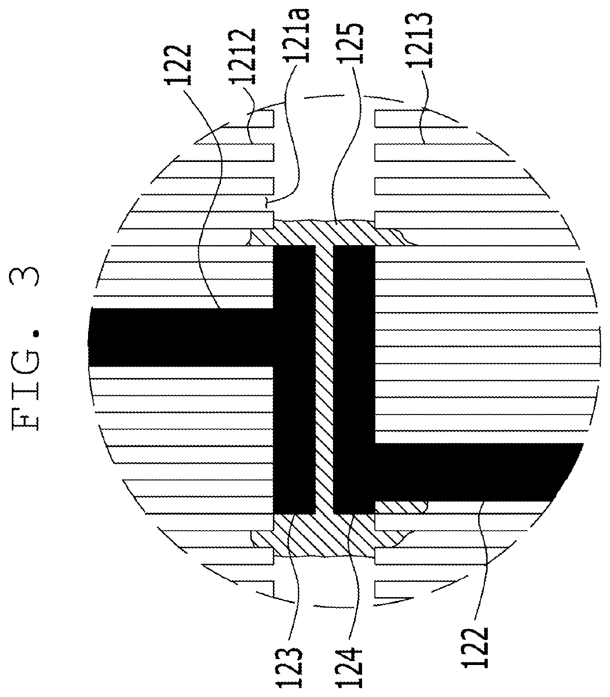
[0030]FIG. 1 is a view schematically showing a...


PUM

PropertyMeasurementUnit
aaaaaaaaaa

Abstract

A multilayer ceramic substrate according to the present invention includes a first insulating portion including a body of a ceramic material, a first via conductor penetrating through the body, and a first internal wiring layer and a first connection pad connected to the first via conductor; and a second insulating portion including a body of an anodized oxide material, a second via conductor penetrating through the body, and a second internal wiring layer and a second connection pad connected to the second via conductor.

Description

CROSS REFERENCE TO RELATED APPLICATION[0001]The present application claims priority to Korean Patent Application No. 10-2019-0013083, filed Jan. 31, 2019, the entire contents of which is incorporated herein for all purposes by this reference.BACKGROUND OF THE INVENTIONField of the Invention[0002]The present invention relates to a multilayer ceramic substrate and a probe card including the same and, more particularly, to a multilayer ceramic substrate having a low thermal expansion coefficient and a high electrical conductivity.Description of the Related Art[0003]In general, the semiconductor fabrication process is performed through a fabrication process of forming a pattern on a wafer, an electrical die sorting (EDS) process of examining electrical characteristics of each chip constituting the wafer, and an assembly process of assembling the patterned wafer into each chip.[0004]Here, the EDS process is performed to determine defective chips among the chips constituting the wafer. In...

Claims


Application Information

Patent Timeline
IPC IPC(8): H01G4/40H01G4/12
CPCH01G4/12H01G4/40H05K1/0271H05K1/0272H05K1/0298H05K1/0306H05K3/4682H05K2201/09227H01G4/232H01G4/30H05K3/4629H05K2203/061H05K2201/096H05K3/4015H05K2201/10303H05K1/115H05K3/4007H05K1/09G01R1/07314G01R31/2886H05K2201/0116
Inventor AHN, BUM MOPARK, SEUNG HOBYUN, SUNG HYUN
Owner POINT ENG
Learn More