
Crystalline film and lighting-emitting device having oriented luminescent emitters

Pending Publication Date: 2020-08-27
MATRIX SENSORS
View PDF1 Cites 4 Cited by
  • Summary
  • Abstract
  • Description
  • Claims
  • Application Information

AI Technical Summary

Benefits of technology

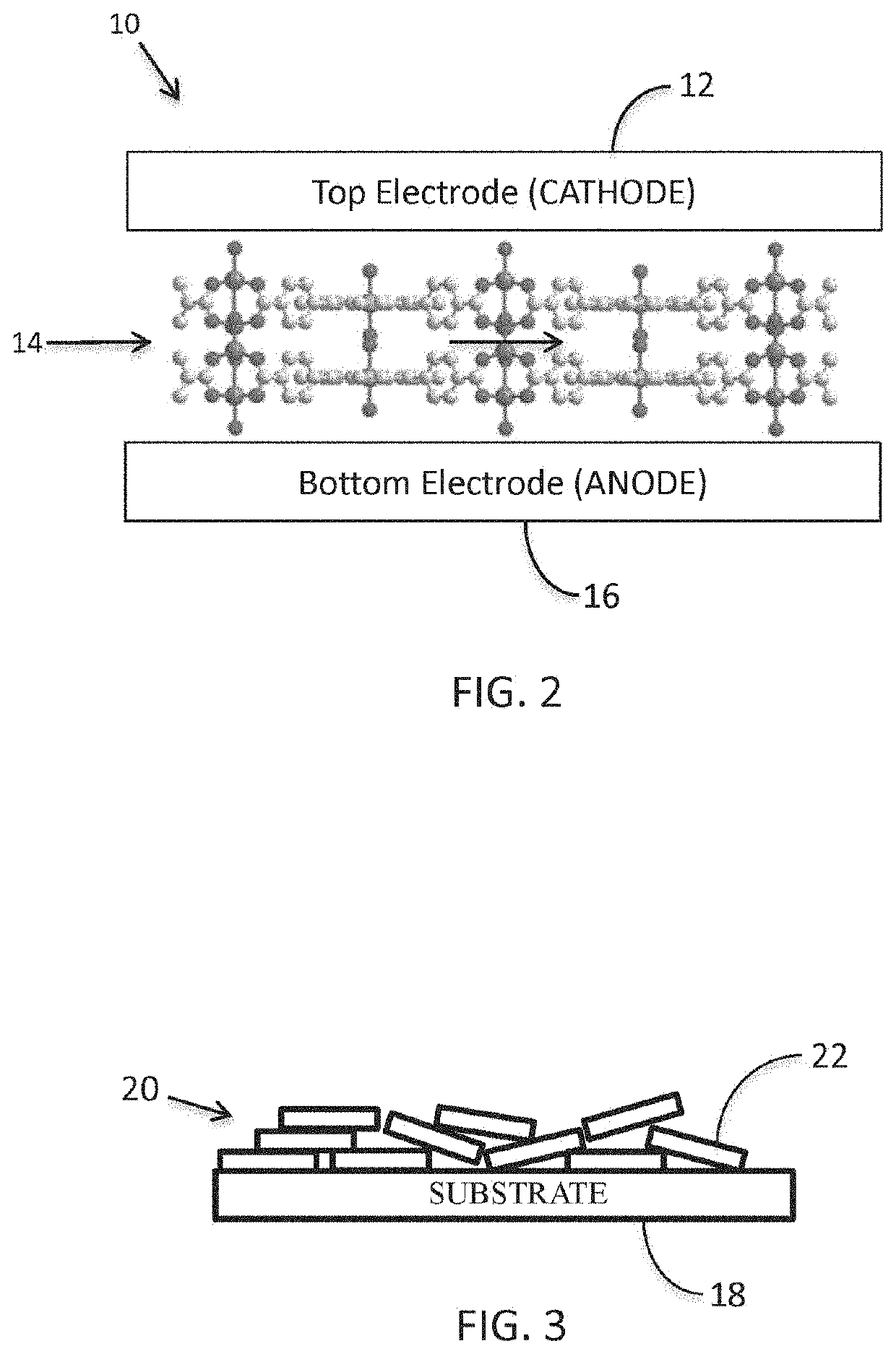
This patent discusses a new way of using a crystalline film in a light-emitting device, such as an OLED. The film contains tiny luminescent molecules that are trapped inside a structure made up of metal and organic materials. This structure makes sure that the luminescent molecules are oriented in a way that allows them to emit light in a way that is efficient for the device. By using this structure, the device can produce light that is oriented parallel to the surface of the film, resulting in up to 50% more light being produced. This invention is a way to create more efficient light-emitting devices.

Problems solved by technology

The lack of order in these amorphous layers is a disadvantage for a variety of physical properties, for example for the important conductivity of the semiconductor layers.
A very specific disadvantage for the efficiency of the components arises, however, in the area of the light-emitting components, more particularly of organic light-emitting diodes.
In these components, the disoriented emission of light harbors a large loss factor for the external quantum efficiency, i.e., the fraction of photons generated that is also actually emitted to the outside.
This solution, however, is not very effective, since the excitation of plasmons in the electrodes means that there are again large losses of the generated light quanta.
A fundamental barrier to the orientation of the emitters, however, is that it is necessary to know the direction in which a molecule is emitting, in relation to its internal molecular coordinate system.

Method used


Image

  • Crystalline film and lighting-emitting device having oriented luminescent emitters
  • Crystalline film and lighting-emitting device having oriented luminescent emitters
  • Crystalline film and lighting-emitting device having oriented luminescent emitters

Examples


example 1

and Methods for Fabricating Cu2(TCPP) Film

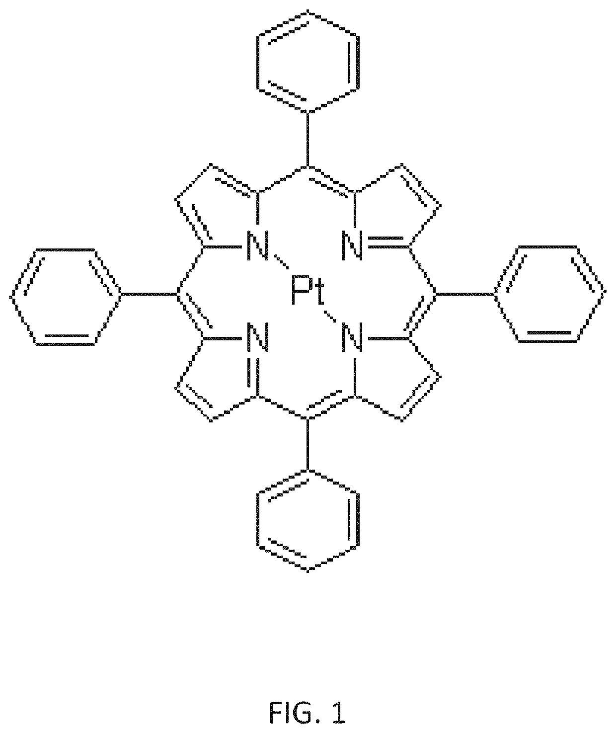
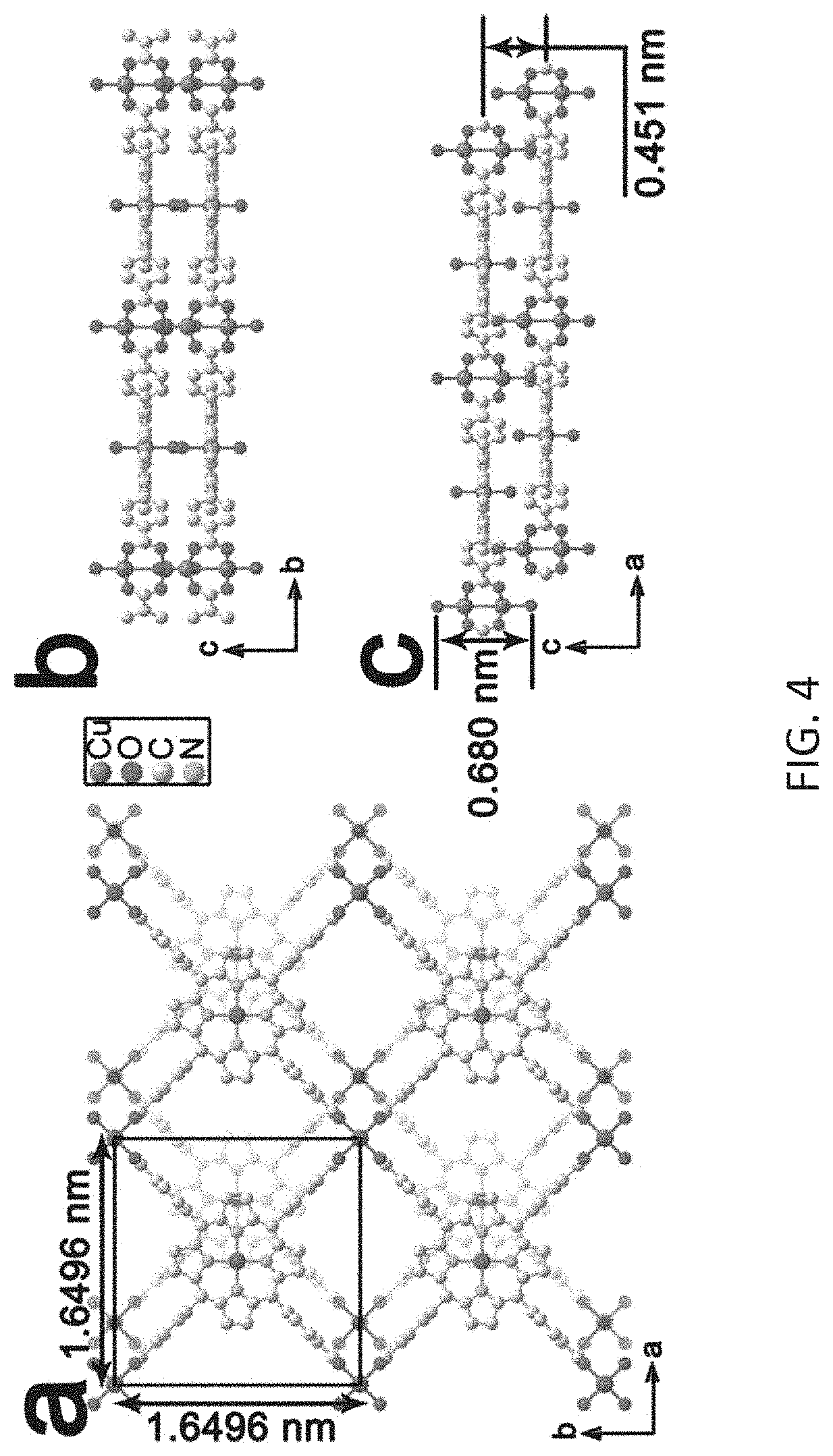
[0176]Copper nitrate trihydrate (7 mg) and 5,10,15,20-tetrakis(4-carboxyphenyl)porphyrin] (TCPP, 30 mg) are dissolved in a solution of 1.5 mL diethylformamide and 0.5 mL ethanol. The resulting solution is sealed in a glass vial and placed in an oven. The oven is heated to 80° C. over a period of 30 minutes and held at 80° C. for a period of 12 hours. The oven is then cooled at a rate of 5° C. / hour to room temperature. The resulting solution is centrifuged. The liquid contents are discarded and the red-brown solid, Cu2(TCPP), is redispersed in 2 mL methanol. The centrifugation process is repeated two times. The resulting solution is diluted in methanol to a desired concentration, which may be one tenth the starting concentration, and deposited as a thin film onto a substrate. Thin film deposition may proceed as follows: The dispersion of Cu2(TCPP) in methanol is pipetted dropwise onto the surface of water in a beaker. The MOF is observed to f...


PUM


Abstract

A film, and a light-emitting device (e.g., an OLED) incorporating the film as an emission layer, have luminescent emitters that are maintained in a desired orientation by incorporating them into a crystalline framework material, such as a metal-organic framework (MOF), covalent organic framework (COF), or porous coordination polymer. The crystal structure in the film has at least one crystallographic axis that is aligned substantially parallel to the planar surface of the film and / or the planar surface of a device substrate on which the film is deposited or grown. The luminescent emitters are held and oriented in the unit cells of the crystalline framework material such that their transition dipoles are substantially parallel to the crystallographic axis, which is in turn substantially parallel to the surface of the film or emission layer of the device through which light is emitted, resulting in improved outcoupling of light.

Description

[0001]This patent application claims the benefit of U.S. provisional patent application 62 / 809,333 filed on Feb. 22, 2019 which application is hereby incorporated by reference in its entirety.FIELD OF THE INVENTION[0002]The present disclosure relates generally to a light-emitting device, such as an organic light-emitting diode (OLED), and a crystalline film suitable for use in an emission layer of the device, in which emitter materials, such as luminescent moieties or molecules, are maintained in a desired orientation by incorporating them into a crystalline framework material (e.g., a metal-organic framework, covalent organic framework, or porous coordination polymer material).INTRODUCTION[0003]Semiconductor layers employed in organic semiconductor components are primarily amorphous. The lack of order in these amorphous layers is a disadvantage for a variety of physical properties, for example for the important conductivity of the semiconductor layers. A very specific disadvantage ...

Claims


Application Information

Patent Timeline
IPC IPC(8): H01L51/00C07D487/22C09K11/06
CPCC09K2211/1029H01L51/5012C09K2211/188C07D487/22C09K11/06H01L51/5016H01L51/0091H10K85/346H10K85/342H10K85/371H10K50/11H10K2101/10
Inventor BRITT, DAVID K
Owner MATRIX SENSORS
Learn More