Sheet for sintering bonding and sheet for sintering bonding with base material

a technology for sintering bonding and sheet metal, which is applied in the direction of film/foil adhesives, manufacturing tools, solventing apparatus, etc., can solve the problem that power semiconductor devices often generate a large amount of heat, and achieve the effect of convenient handling

Pending Publication Date: 2020-09-17
NITTO DENKO CORP
View PDF3 Cites 1 Cited by
  • Summary
  • Abstract
  • Description
  • Claims
  • Application Information

AI Technical Summary

Benefits of technology

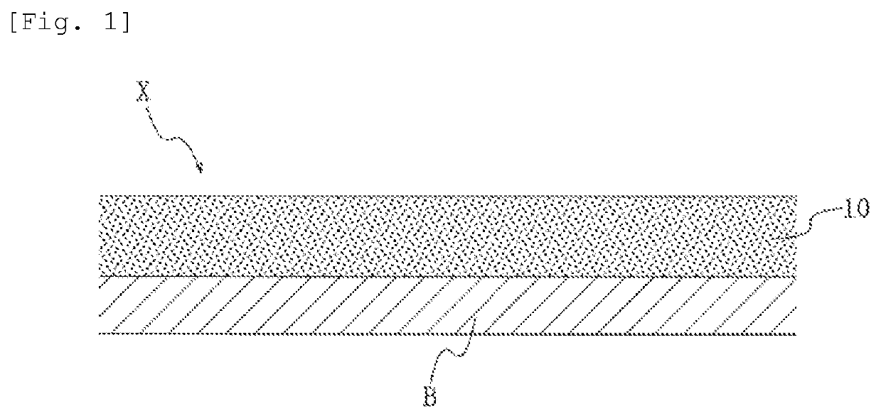
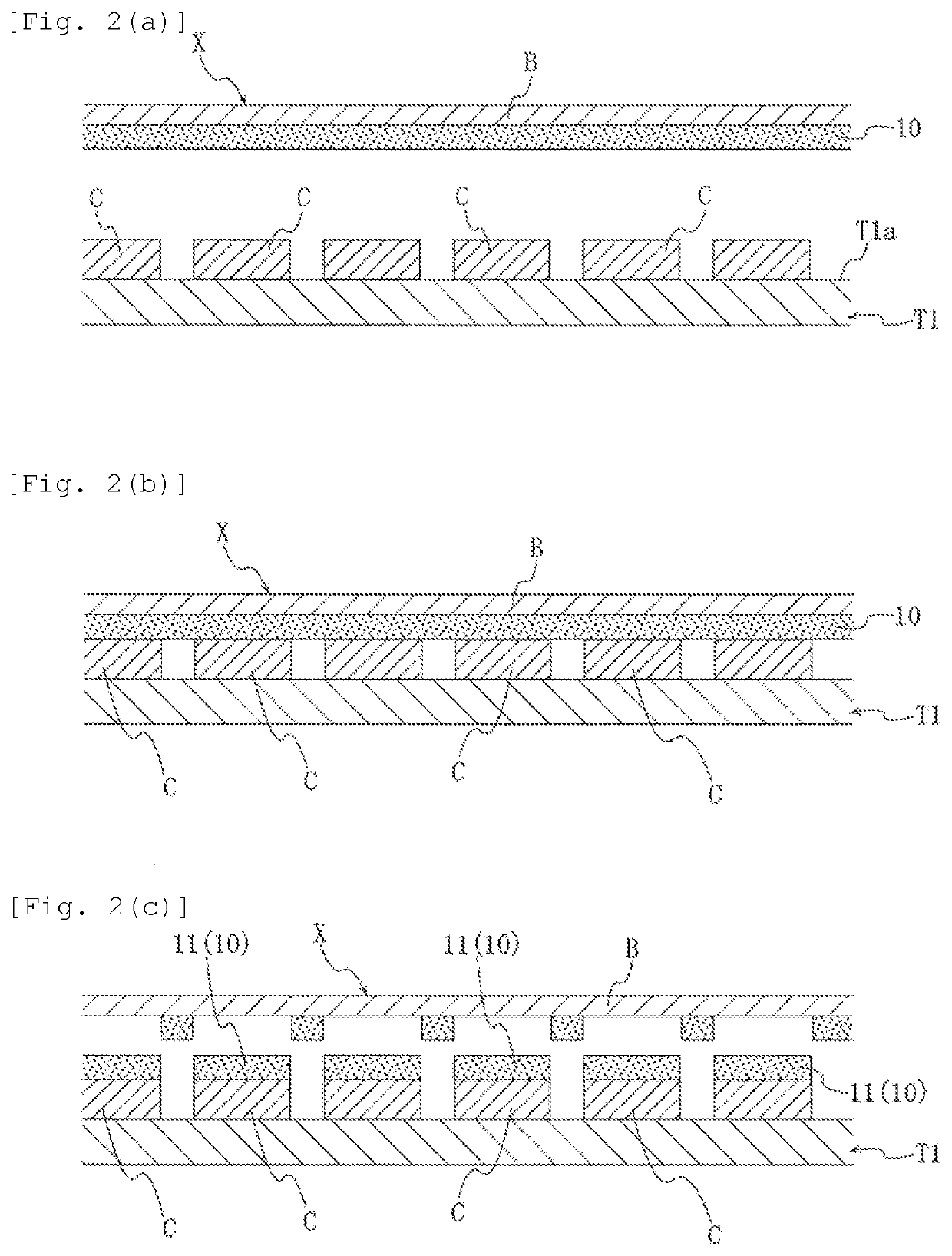
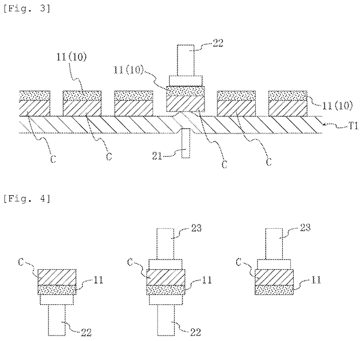
[0025]According to the second aspect of the present invention, a sheet for sintering bonding with a base material is provided. This sheet for sintering bonding with a base material has a laminated structure comprising a base material and the sheet for sintering bonding mentioned above according to the first aspect of the present invention. As such, the sheet for sintering bonding according to the present invention may be accompanied by a base material. Such a sheet for sintering bonding with a base material is easily handled, and according to the sheet for sintering bonding with a base material, for example, it is easy to perform the transfer step mentioned above in which the lamination operation and the subsequent separation operation are carried out.

Problems solved by technology

Power semiconductor devices often generate a large amount of heat due to a large amount of energization upon operation.

Method used


Image

  • Sheet for sintering bonding and sheet for sintering bonding with base material
  • Sheet for sintering bonding and sheet for sintering bonding with base material
  • Sheet for sintering bonding and sheet for sintering bonding with base material

Examples


example 1

[0075]By using a hybrid mixer (trade name: “HM-500”, manufactured by Keyence Corporation) at its stirring mode, 56.35 parts by mass of a silver particle as a sinterable particle P1, 1.7 parts by mass of a polycarbonate resin as a high molecular binder (a thermally decomposable high molecular binder) (trade name: “QPAC 40”, the weight average molecular weight is 150000, solid at ordinary temperature, manufactured by Empower Materials), 2.55 parts by mass of isobornyl cyclohexanol as a low molecular binder (a low boiling point binder) (trade name: “Terusolve MTPH”, liquid at ordinary temperature, manufactured by NIPPON TERPENE CHEMICALS, INC.), and 39.4 parts by mass of methyl ethyl ketone as a solvent were mixed to prepare a varnish. The stirring time was set to be 3 minutes. The above silver particle as the sinterable particle P1 comprises the first silver particle (the average particle diameter: 60 nm, manufactured by DOWA Electronics Materials Co., Ltd.) and the second silver part...

example 2

[0076]A sheet for sintering bonding of Example 2 was made in the same manner as the sheet for sintering bonding of Example 1 except that the amount of the sinterable particle P1 to be compounded was changed from 56.35 parts by mass to 56.16 parts by mass; the amount of the polycarbonate resin (trade name: “QPAC 40”, manufactured by Empower Materials) to be compounded was changed from 1.7 parts by mass to 2.63 parts by mass; the amount of isobornyl cyclohexanol (trade name: “Terusolve MTPH”, manufactured by NIPPON TERPENE CHEMICALS, INC.) to be compounded was changed from 2.55 parts by mass to 1.76 parts by mass; and the amount of methyl ethyl ketone to be used was changed from 39.4 parts by mass to 39.45 parts by mass. With respect to the sheet for sintering bonding of Example 2, the content of the sinterable particle is 92.7% by mass, and the thickness is 52 μm.

example 3

[0077]A sheet for sintering bonding of Example 3 was made in the same manner as the sheet for sintering bonding of Example 1 except that the amount of the sinterable particle P1 to be compounded was changed from 56.35 parts by mass to 56.98 parts by mass; the amount of the polycarbonate resin (trade name: “QPAC 40”, manufactured by Empower Materials) to be compounded was changed from 1.7 parts by mass to 0.75 parts by mass; the amount of isobornyl cyclohexanol (trade name: “Terusolve MTPH”, manufactured by NIPPON TERPENE CHEMICALS, INC.) to be compounded was changed from 2.55 parts by mass to 2.98 parts by mass; and the amount of methyl ethyl ketone to be used was changed from 39.4 parts by mass to 39.29 parts by mass. With respect to the sheet for sintering bonding of Example 3, the content of the sinterable particle is 93.9% by mass, and the thickness is 53 μm.


PUM

PropertyMeasurementUnit
shear strengthaaaaaaaaaa
widthaaaaaaaaaa

Abstract

To provide a sheet for sintering bonding and a sheet for sintering bonding with a base material that are suited for being made with a good operational efficiency and that are also suited for realizing a satisfactory operational efficiency in a sintering process in a process of producing a semiconductor device that goes through sintering bonding of semiconductor chips. A sheet for sintering bonding 10 of the present invention comprises an electrically conductive metal containing sinterable particle and a binder component, and has a shear strength at 23° C. of 2 to 40 MPa measured in accordance with a SAICAS method. A sheet body X, which is a sheet for sintering bonding with a base material according to the present invention, has a laminated structure comprising a base material B and the sheet for sintering bonding 10.

Description

TECHNICAL FIELD[0001]The present invention relates to a sheet for sintering bonding that can be used for producing semiconductor devices and the like, and a sheet for sintering bonding accompanied by a base material.BACKGROUND ART[0002]In production of semiconductor devices, as a technique for die bonding a semiconductor chip to a supporting substrate, such as a lead frame or an insulating circuit substrate, while making an electrical connection with the side of the supporting substrate, a technique for forming a Au—Si eutectic alloy layer between the supporting substrate and the chip to realize a bonded state, or a technique for utilizing solder or an electrically conductive particle containing resin as a bonding material have been known.[0003]Meanwhile, the spread of power semiconductor devices playing a role of controlling power supply has been remarkable in recent years. Power semiconductor devices often generate a large amount of heat due to a large amount of energization upon ...

Claims


Application Information

Patent Timeline
Patent Type & Authority Applications(United States)
IPC IPC(8): H01L23/00
CPCH01L24/83H01L24/27H01L2224/27505H01L2224/8384C09J7/30C09J9/02C09J169/00C09J11/06H01L23/488H01L24/29C08K2003/0806C09J2469/00H01L2224/29099C08K3/08C08K5/05H01L2224/27436H01L2224/27002H01L2224/27003H01L2224/05639H01L2224/04026H01L2224/83907H01L2224/29339H01L2224/29347H01L2224/29387H01L2224/29344H01L2224/29364H01L2224/29311H01L2224/29355H01L2224/29444H01L2224/29439H01L2224/83439H01L2224/83055H01L2224/83065H01L2224/2939H01L2224/05166H01L2224/05073H01L2224/0345H01L2224/95H01L24/03H01L24/95H01L2224/32245H01L2224/32227H01L2224/83444H01L2224/83455H01L2224/83464H01L2224/83469H01L2224/83203H01L2224/83075H01L24/85H01L2224/85205H01L2224/85207H01L2224/45144H01L2224/45124H01L2224/45147H01L24/92H01L2224/97H01L24/97H01L2224/92247H01L2224/73265H01L2224/271H01L24/05H01L24/32H01L24/73H01L2924/181H01L2924/10272H01L2924/1033B23K35/0244H01L2924/00014H01L2924/0541H01L2924/01047H01L2924/01029H01L2924/054H01L2924/01046H01L2924/0544H01L2924/0105H01L2224/27H01L2924/00012H01L2224/83H01L2224/85
Inventor MITA, RYOTAICHIKAWA, TOMOAKI
Owner NITTO DENKO CORP
Why Eureka
Try Eureka