Graphene-semiconductor heterojunction photodetector and method of manufacturing the same

a graphene-semiconductor and photodetector technology, applied in the direction of semiconductor devices, basic electric elements, electrical apparatus, etc., can solve the problems of low photoresponsivity, the height of a schottky barrier cannot be precisely controlled, and the fermi level of the graphene layer cannot be controlled precisely, so as to achieve high output voltage, high photosensitivity, and high output voltage

Active Publication Date: 2020-11-05
GWANGJU INST OF SCI & TECH
View PDF0 Cites 4 Cited by
  • Summary
  • Abstract
  • Description
  • Claims
  • Application Information

AI Technical Summary

Benefits of technology

[0040]According to the present inventive concept, a source electrode and a test electrode are formed to face each other on a graphene layer, and a drain electrode is formed in a direction perpendicular to a central region portion of the graphene layer, so that the drain electrode can be physically separated from the graphene layer.
[0041]Further, charges formed at the central region portion of the graphene layer are transmitted to the drain electrode through a substrate, so that high photosensitivity can be secured, and a high output voltage can be secured for the applied light. Accordingly, the drain electrode is formed at a side surface of the graphene layer, so that the size of the drain electrode can be easily controlled, and a high output voltage can be obtained.
[0042]Further, an intermediate layer is formed between the heterojunction components, the substrate and the graphene layer, so that, due to the asymmetric tunneling effect at the interface, electron injection can decrease and hole injection can increase. Accordingly, an energy barrier increases by the intermediate layer to decrease a dark current, and as the dark current decreases, photodetection efficiency can be improved.
[0043]Further, electron-hole pairs are formed in semiconductors as well as graphene, so that the photoabsorption rate and photoresponsivity of the photodetector increase, and photoelectric conversion gain that increases or decreases photoresponsivity is generated according to a gate voltage. By utilizing these, there is an advantage in that the photoresponsivity can be improved or the photoresponsivity can be controlled according to the application
[0044]In addition, in a graphene-semiconductor heterojunction photodetector having an array form, the source electrodes are each formed on each of the graphene layers in the form of an array, and one drain electrode is formed in a direction perpendicular to the graphene layers in the form of an array and the source electrodes, so that the drain electrode can be commonly used. That is, as the drain electrode is commonly used, a light-receiving area per unit area of the photodetector can increase.
[0045]Further, the drain electrode is formed to extend along the entire width of an array of the source electrodes, so that wiring between the drain electrode and the desired source electrode can be selectively performed. Thus, an operating point can be randomly changed according to the wiring of the desired source electrode.

Problems solved by technology

However, there is a limitation in controlling the Fermi level of the graphene layer 20 because the silicon substrate 10 itself acts as a portion of the gate electrode 60 or the gate electrode 60 acts on the rear surface thereof.
In addition, the height of a Schottky barrier may not be precisely controlled, and thus there is a disadvantage of exhibiting low photoresponsivity.

Method used


Image

  • Graphene-semiconductor heterojunction photodetector and method of manufacturing the same
  • Graphene-semiconductor heterojunction photodetector and method of manufacturing the same
  • Graphene-semiconductor heterojunction photodetector and method of manufacturing the same

Examples


first embodiment

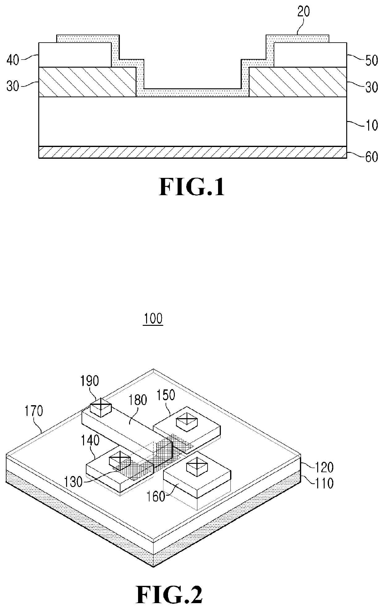
[0069]Referring to FIG. 2, a photodetector 100 according to the present inventive concept includes a substrate 110, an insulating layer 120, a graphene layer 130, a source electrode 140, a test electrode 150, a drain electrode 160, a gate insulating layer 170, and a gate electrode 180.

[0070]The substrate 110 may be a doped semiconductor substrate 110. For example, the substrate 110 may be a p-type or n-type impurity-doped substrate 110, and may preferably be an n-type doped substrate 110. In addition, the substrate 110 may include silicon (Si) or germanium (Ge), but is not limited thereto, and may have other semiconductor materials doped with an n-type impurity.

[0071]The insulating layer 120 is formed on the substrate 110 and serves as an insulating film for insulating the source electrode 140 and the test electrode 150, which will be described later. The insulating layer 120 is preferably made of silicon nitride, silicon oxide, or the like, but may be made of any material as long a...

fourth embodiment

[0110]Referring to FIG. 8, the present inventive concept illustrates a graphene-semiconductor heterojunction photodetector in the form of an array.

[0111]That is, a graphene-semiconductor heterojunction photodetector 400 with the form of an array according to the fourth embodiment of the present inventive concept includes a substrate 110, an insulating layer 120, graphene layers 130 in the form of an array, source electrodes 140, a drain electrode 160, a gate insulating layer 170, and gate electrodes 180.

[0112]The substrate 110 may be a doped semiconductor substrate 110. For example, the substrate 110 may be a p-type or n-type impurity-doped substrate 110, and preferably, may be an n-type doped substrate 110. In addition, the substrate 110 may include Si or Ge, but is not limited thereto, and may have other semiconductor materials doped with an n-type impurity.

[0113]The insulating layer 120 is formed on the substrate 110 and serves as an insulating film for insulating the source elec...

second embodiment

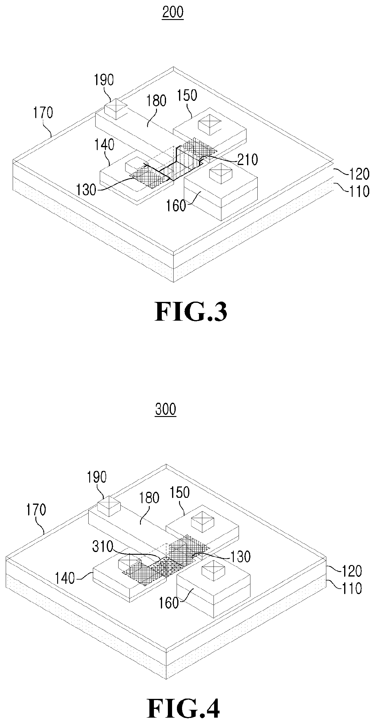
[0163]FIG. 19 is a view illustrating a method of manufacturing the photodetector according to the present inventive concept.

[0164]Referring to FIG. 19, a manufacturing method of the photodetector 200 according to the second embodiment of the present inventive concept is the same as the manufacturing method of the photodetector 100 according to the first embodiment until after the operations of the manufacturing method illustrated with reference to FIGS. 11 to 15. That is, the manufacturing method has the same operations until after the operations of forming an insulating layer 120 on a substrate 110, forming a graphene layer 130 on the substrate 110 and the insulating layer 120, and then forming a source electrode 140, a test electrode 150, and a drain electrode 160 on the graphene layer 130 and the substrate 110. Thereafter, forming a dopant layer 210 on an exposed portion of the graphene layer 130 may be further included. That is, as shown in FIG. 19, an exposed surface of the gra...


PUM

PropertyMeasurementUnit
dark current characteristicsaaaaaaaaaa
dark currentaaaaaaaaaa
semiconductoraaaaaaaaaa

Abstract

In a graphene-semiconductor heterojunction photodetector and a method of manufacturing the same according to the present inventive concept, a source electrode and a test electrode are formed to face each other on a graphene layer, and a drain electrode is formed in a direction perpendicular to a central region portion of the graphene layer, so that the drain electrode may be physically separated from the graphene layer. Further, charges formed at the central region portion of the graphene layer are transmitted to the drain electrode through a substrate, so that high photosensitivity may be secured, and a high output voltage may be secured for the applied light. Accordingly, the drain electrode is formed at a side surface of the graphene layer, so that the size of the drain electrode may be easily controlled, and a high output voltage may be obtained.

Description

CLAIM FOR PRIORITY[0001]This application claims priority to Korean Patent Application No. 2019-0052549 filed on May 3, 2019 and No. 2019-0052555 filed on May 3, 2019 in the Korean Intellectual Property Office (KIPO), the entire contents of which are hereby incorporated by reference.BACKGROUND1. Technical Field[0002]Example embodiments of the present disclosure relate to a graphene-semiconductor heterojunction photodetector and a method of manufacturing the same, and more specifically, to a graphene-semiconductor heterojunction photodetector capable of adjusting gain by applying a gate voltage and improving photodetection efficiency, and a method of manufacturing the same.2. Related Art[0003]Graphene is a sheet-shaped material composed of sp2 bonded carbon atoms and has a characteristic of zero band gap. That is, the graphene has characteristics in which band gap thereof is close to zero, and conduction and valence bands have a conical shape within an extremely low range with respect...

Claims


Application Information

Patent Timeline
Patent Type & Authority Applications(United States)
IPC IPC(8): H01L31/0216H01L31/0224H01L31/028H01L31/113H01L31/18
CPCH01L31/1136H01L31/02162H01L31/1804H01L31/0224H01L31/028
Inventor LEE, BYOUNG HUNCHANG, KYOUNG EUN
Owner GWANGJU INST OF SCI & TECH
Why Eureka
Try Eureka