Supercharge Your Innovation With Domain-Expert AI Agents!

Fabrication method for fused multi-layer amorphous selenium sensor

a technology of amorphous selenium and amorphous selenium, which is applied in the field of sensor, can solve the problems of increasing the cost of the imager, reducing the effect of the imager, and reducing the efficiency of the imager

Active Publication Date: 2020-11-12
THE RES FOUND OF STATE UNIV OF NEW YORK
View PDF0 Cites 0 Cited by
  • Summary
  • Abstract
  • Description
  • Claims
  • Application Information

AI Technical Summary

Benefits of technology

This approach results in reliable multi-layer sensors with enhanced signal amplification and reduced electronic noise, improving the performance of optical and x-ray detectors by forming efficient charge blocking layers without crystallization, leading to improved image quality and sensitivity.

Problems solved by technology

As will be appreciated, conventional x-ray detectors, especially x-ray detectors adapted for low photon flux applications, suffer from image degradation due to electronic noise.
However, decreasing the electronic noise of readout electronics increases the cost of the imager and has limited effect.

Method used


Image

  • Fabrication method for fused multi-layer amorphous selenium sensor
  • Fabrication method for fused multi-layer amorphous selenium sensor
  • Fabrication method for fused multi-layer amorphous selenium sensor

Examples


Embodiment Construction

[0026]Reference will now be made in greater detail to various embodiments of the subject matter of the present application, some embodiments of which are illustrated in the accompanying drawings. The same reference numerals will be used throughout the drawings to refer to the same or similar parts.

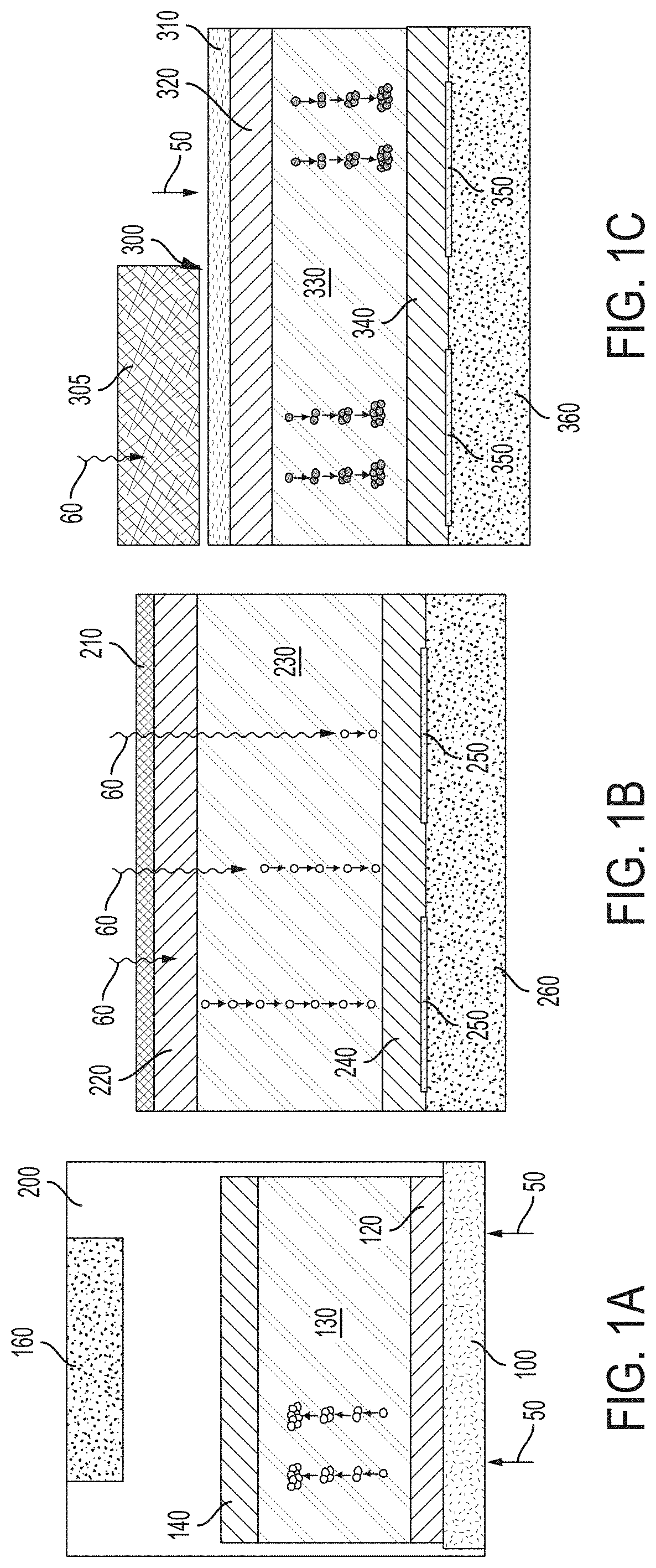
[0027]Schematic diagrams of an example optical sensor, direct x-ray detector, and indirect x-ray detector are shown in FIG. 1A, FIG. 1B and FIG. 1C, respectively.

[0028]Referring to FIG. 1A, an optical sensor includes a transparent substrate 100 such as an electroded glass substrate. The high voltage electrode (not separately shown) can be formed on the substrate from a suitable transparent, conductive material such as indium tin oxide (ITO) using conventional deposition and patterning techniques such as physical vapor deposition (e.g., evaporation or sputtering) and photolithography.

[0029]A first charge blocking layer 120 is formed over the substrate 100. First charge blocking layer 120 ma...


PUM

PropertyMeasurementUnit
electric fieldsaaaaaaaaaa
temperatureaaaaaaaaaa

Abstract

A sensor including a layer of amorphous selenium (a-Se) and at least one charge blocking layer is formed by depositing the charge blocking layer over a substrate prior to depositing the amorphous selenium, enabling the charge blocking layer to be formed at elevated temperatures. Such a process is not limited by the crystallization temperature of a-Se, resulting in the formation of an efficient charge blocking layer, which enables improved signal amplification of the resulting device. The sensor can fabricated by forming first and second amorphous selenium layers over separate substrates, and then fusing the a-Se layers at a relatively low temperature.

Description

CROSS REFERENCE TO RELATED APPLICATIONS[0001]The present application is a continuation of co-pending application having U.S. Ser. No. 16 / 715,023, filed on Dec. 16, 2019, which is a continuation of co-pending application having U.S. Ser. No. 15 / 761,187, filed on Mar. 19, 2018, now U.S. Pat. No. 10,547,015, which is a 371 of International Application having Serial No. PCT / US2017 / 063857, filed on Nov. 30, 2017, which claims the benefit of priority from U.S. Provisional Application No. 62 / 429,101, filed on Dec. 2, 2016, the content of which is incorporated herein by reference in its entirety.GOVERNMENT LICENSE RIGHTS[0002]This invention was made with government support under grant number EB002655 awarded by the National Institutes of Health. The government has certain rights in the invention.BACKGROUND OF THE INVENTION[0003]The present application relates generally to sensors adapted to detect optical or ionizing radiation, and more specifically to multi-layer amorphous selenium (a-Se) ...

Claims


Application Information

Patent Timeline
Patent Type & Authority Applications(United States)
IPC IPC(8): H01L51/42G01T1/20G01T1/24H01L27/30
CPCH01L27/307G01T1/2018H01L2031/0344G01T1/241H01L27/308H01L51/4213G01T1/247H01L31/0272H01L27/14663H01L27/14676H01L27/14696H01L31/115G01T1/20G01T1/24Y02E10/549H10K30/10H10K30/50H10K39/32H10K39/36
Inventor SCHEUERMANN, JAMESZHAO, WEI
Owner THE RES FOUND OF STATE UNIV OF NEW YORK
Features
  • R&D
  • Intellectual Property
  • Life Sciences
  • Materials
  • Tech Scout
  • Unparalleled Data Quality
  • Higher Quality Content
  • 60% Fewer Hallucinations
Learn More