Charged Particle Beam Device
- Summary
- Abstract
- Description
- Claims
- Application Information
AI Technical Summary
Benefits of technology
Problems solved by technology
Method used
Image
Examples
first embodiment
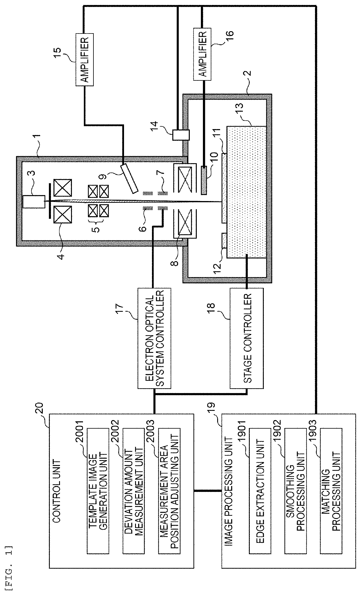
[0038]First, a schematic configuration of a scanning electron microscope (SEM) as a charged particle beam device according to a first embodiment will be described with reference to FIG. 1. This SEM includes a column 1 which is an electron optical system, and a sample chamber 2.
[0039]The column 1 includes an electron gun 3 for generating an electron beam (charged particle beam) to be irradiated, a condenser lens 4, an aligner 5, an ExB filter 6, a deflector 7, and an objective lens 8, and functions as a charged particle beam irradiation unit. The condenser lens 4 and the objective lens 8 focus the electron beam generated by the electron gun 3 and irradiate a wafer 11 as a sample with the electron beam. The deflector 7 deflects the electron beam according to the applied voltage in order to scan the electron beam on the wafer 11. The aligner 5 is configured to generate an electric field for aligning the electron beam with respect to the objective lens 8. The ExB filter 6 is a filter fo...
second embodiment
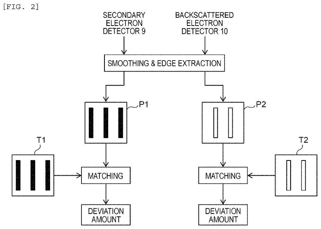
[0084]Next, a scanning electron microscope (SEM) as a charged particle beam device according to a second embodiment of the present invention will be described with reference to FIGS. 10 to 17. The device of the second embodiment is similar to that of the first embodiment in that the template image T1 for a secondary electron image and the template image T2 for a backscattered electron image are used. This embodiment is different from the first embodiment in a user interface screen for registering a template image and the like.
[0085]In the second embodiment, for convenience of description, a case where a pattern is formed over three layers on the wafer 11 as shown in FIG. 10 will be described as an example. However, it is needless to say that the device of the second embodiment is not limited to the measurement of a wafer having such a structure. FIG. 10(a) is a plan view of the wafer 11 viewed from the irradiation direction of the irradiation electrons, and FIG. 10 (b) is a cross-se...
third embodiment
[0118]Next, a scanning electron microscope (SEM) as a charged particle beam device according to a third embodiment of the present invention will be described with reference to FIGS. 18 to 22. The device according to the third embodiment is similar to that of the above-described embodiments in that the template image T1 for the secondary electron image (first image P1) and the template image T2 for the backscattered electron image (second image P2) are used. This embodiment is different from the above-described embodiments in the method for registering a template image.
[0119]FIG. 18 shows an example of the configuration of the wafer 11 to be measured in the device according to the third embodiment. FIG. 18 (a) is a front view of the wafer 11 viewed from the incident direction of the irradiation electrons, and FIG. 18 (b) shows a cross section taken along the line F-F′ of FIG. 18 (a).
[0120]A pattern 201 having a vertical direction as a longitudinal direction is formed on the surface o...
PUM
 Abstract
Description
Claims
Application Information


