Semiconductor structure and formation method thereof

Inactive Publication Date: 2020-12-24
SEMICON MFG INT (SHANGHAI) CORP +1
View PDF0 Cites 0 Cited by
  • Summary
  • Abstract
  • Description
  • Claims
  • Application Information

AI Technical Summary

Benefits of technology

[0028]In embodiments and implementations of the present disclosure, a seed layer is formed on the bottom and sidewall of a contact hole, and the thickness of the seed layer on the bottom of the contact hole is greater than the thickness of the seed layer on the sidewall of the contact hole, so that when a conductive plug is formed in the contact hole, since the thickness of the seed layer on the bottom of the contact hole is large, a conductive material is relatively easy to nucleate on the thicker seed layer. Therefore, the growth rate of the conductive material a

Problems solved by technology

With the development trend of the very-large-scale integrated circuits, integrated circuits are becoming more and more complex, and semiconductor device technology nodes are continuously decreasing.
When a size of a semiconductor device is reduced to a ce

Method used


Image

  • Semiconductor structure and formation method thereof
  • Semiconductor structure and formation method thereof
  • Semiconductor structure and formation method thereof

Examples


Example

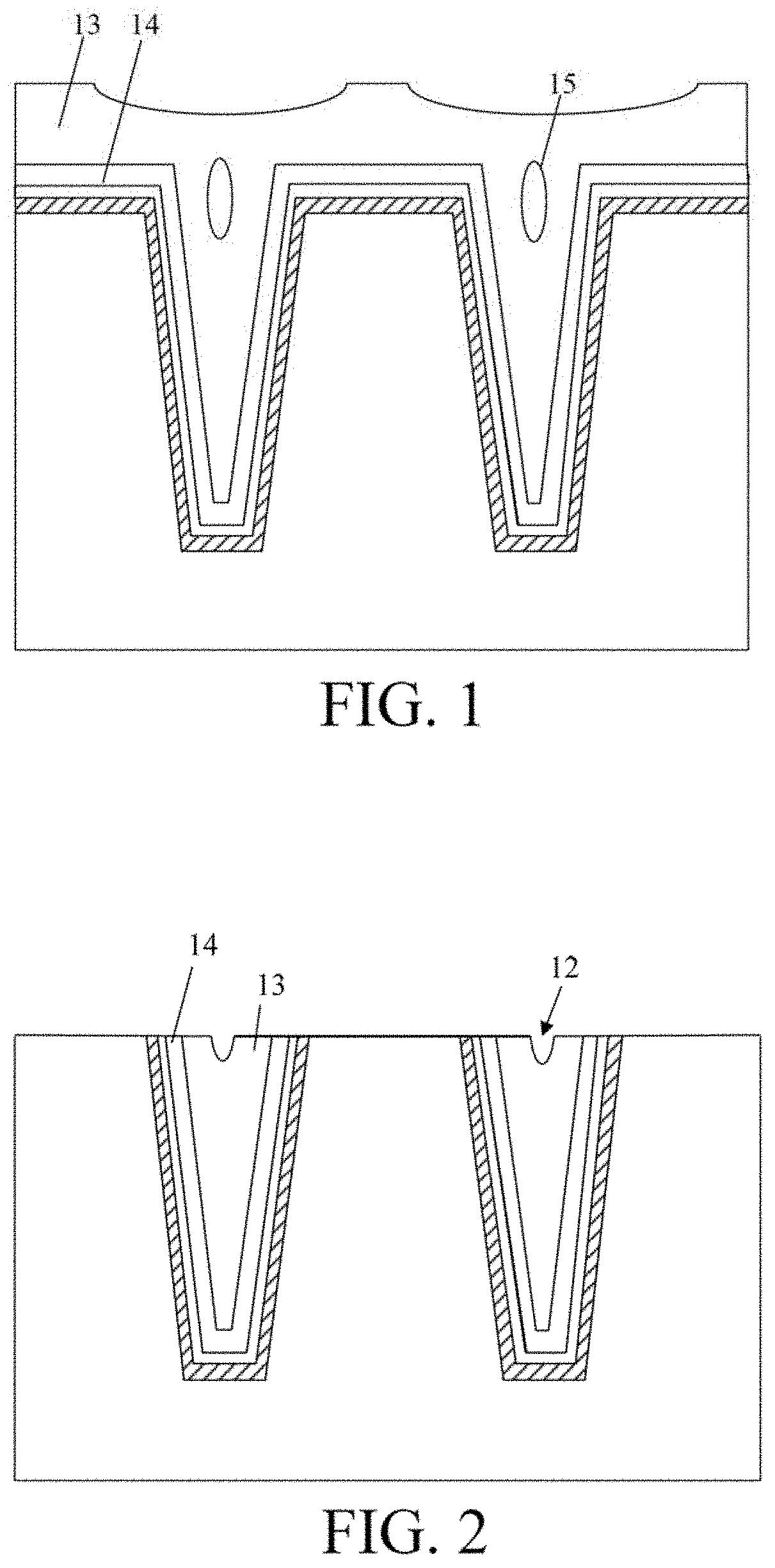
[0031]It is known from the background art that a contact hole plug and an external circuit have a problem of low electrical connection reliability. The cause of the problem is illustrated in conjunction with a schematic diagram of a formation method of a semiconductor structure shown in FIG. 1 and FIG. 2.

[0032]Referring to FIG. 1, an opening of a contact hole is decreasing in size, and a seed layer 14 is formed on a sidewall and bottom of the contact hole. When a conductive material 13 is filled into the contact hole by electroplating, while the conductive material on the bottom of the contact hole has not yet grown to the desired thickness, the conductive material on the sidewall of the contact hole has filled the opening of the contact hole, so as to generate a hole 15 at the opening of the contact hole.

[0033]Referring to FIG. 2, when the excess conductive material 13 is removed by a planarization process, the conductive material 13 remaining in the contact hole remains as a conta...


PUM


Abstract

A semiconductor structure and a formation method thereof are provided. A form of the formation method of the semiconductor structure includes: providing a substrate; forming a dielectric layer on the substrate; forming a contact hole in the dielectric layer; forming a seed layer on a bottom and a sidewall of the contact hole, where a thickness of the seed layer on the bottom of the contact hole is greater than a thickness of the seed layer on the sidewall of the contact hole; and forming a conductive plug in the contact hole. The semiconductor structure includes: a substrate; a dielectric layer located on the substrate; a contact hole located in the dielectric layer; a seed layer located on a bottom and a sidewall of the contact hole, where a thickness of the seed layer on the bottom of the contact hole is greater than a thickness of the seed layer on the sidewall of the contact hole; and a conductive plug located in the contact hole. The present disclosure can improve the reliability of an electrical connection of the conductive plug.

Description

RELATED APPLICATIONS[0001]The present application claims priority to Chinese Patent Appln. No. 201910527770.4, filed Jun. 18, 2019, the entire disclosure of which is hereby incorporated by reference.BACKGROUNDTechnical Field[0002]Embodiments and implementations of the present disclosure relate to the field of semiconductor manufacturing, and in particular, to a semiconductor structure and a formation method thereof.Related Art[0003]Main semiconductor devices of integrated circuits, especially very-large-scale integrated circuits, are metal-oxide-semiconductor field effect transistors (MOS transistors). With the development trend of the very-large-scale integrated circuits, integrated circuits are becoming more and more complex, and semiconductor device technology nodes are continuously decreasing. When a size of a semiconductor device is reduced to a certain extent, various secondary effects occur one after another due to physical limits of the semiconductor device such as large lea...

Claims


Application Information

Patent Timeline
IPC IPC(8): H01L21/768H01L23/532
CPCH01L23/53238H01L21/76802H01L21/76846H01L21/76873H01L21/76847H01L21/76877H01L21/2855H01L21/28556H01L21/76843H01L2221/1089
Inventor JIQUAN, LIU
Owner SEMICON MFG INT (SHANGHAI) CORP
Why Eureka
Try Eureka