Tomography Based Semiconductor Measurements Using Simplified Models

a simplified model and semiconductor technology, applied in the field of metalrology systems and methods, can solve the problems of limiting measurement performance, unrealistic and inaccurate measurement, and raw measurement signals cannot be used to directly determine the physical properties of specimens, etc., and achieves accurate reconstruction of measured structures, reduced data acquisition requirements, and less computational effort

Active Publication Date: 2021-06-03
KLA TENCOR TECH CORP
View PDF9 Cites 1 Cited by
  • Summary
  • Abstract
  • Description
  • Claims
  • Application Information

AI Technical Summary

Benefits of technology

[0010]Methods and systems for improved regularization associated with tomographically resolved image based measurements of semiconductor structures are presented herein. More specifically, the regularizations described herein are based on data (e.g., simulated data, real data, or both) and parameterization of a constrained voxel model that captures known process variations. The constrained voxel model is determined based on simplified geometric models, process models, or both, characterizing the structure under measurement. Regularization based on a constrained voxel model that accurately represents process variations enables convergence to a more accurate reconstruction of the measured structure with less computational effort. This enables semiconductor measurements with reduced data acquisition requirements, e.g., fewer measured angles, and reduced move-acquire-move (MAM) times.

Problems solved by technology

In most cases, the raw measurement signals cannot be used to directly determine the physical properties of the specimen.
Unfortunately, typical, generic regularization employed in tomographic analysis (e.g., total variation regularization, L1 regularization, etc.) limit measurement performance.
In some examples, the application of generic regularization terms is weak, allowing the optimization to fall into local minima and leading to unrealistic and inaccurate measurement results.
In some examples, the application of generic regularization terms results in excessively strong regularization leading to measurement results that lack sufficient detail.
Future metrology applications present challenges for metrology due to increasingly small resolution requirements, multi-parameter correlation, increasingly complex geometric structures, and increasing use of opaque materials.
This often leads to convergence in local minima and incorrect reconstruction.

Method used


Image

  • Tomography Based Semiconductor Measurements Using Simplified Models
  • Tomography Based Semiconductor Measurements Using Simplified Models
  • Tomography Based Semiconductor Measurements Using Simplified Models

Examples


Embodiment Construction

[0036]Reference will now be made in detail to background examples and some embodiments of the invention, examples of which are illustrated in the accompanying drawings.

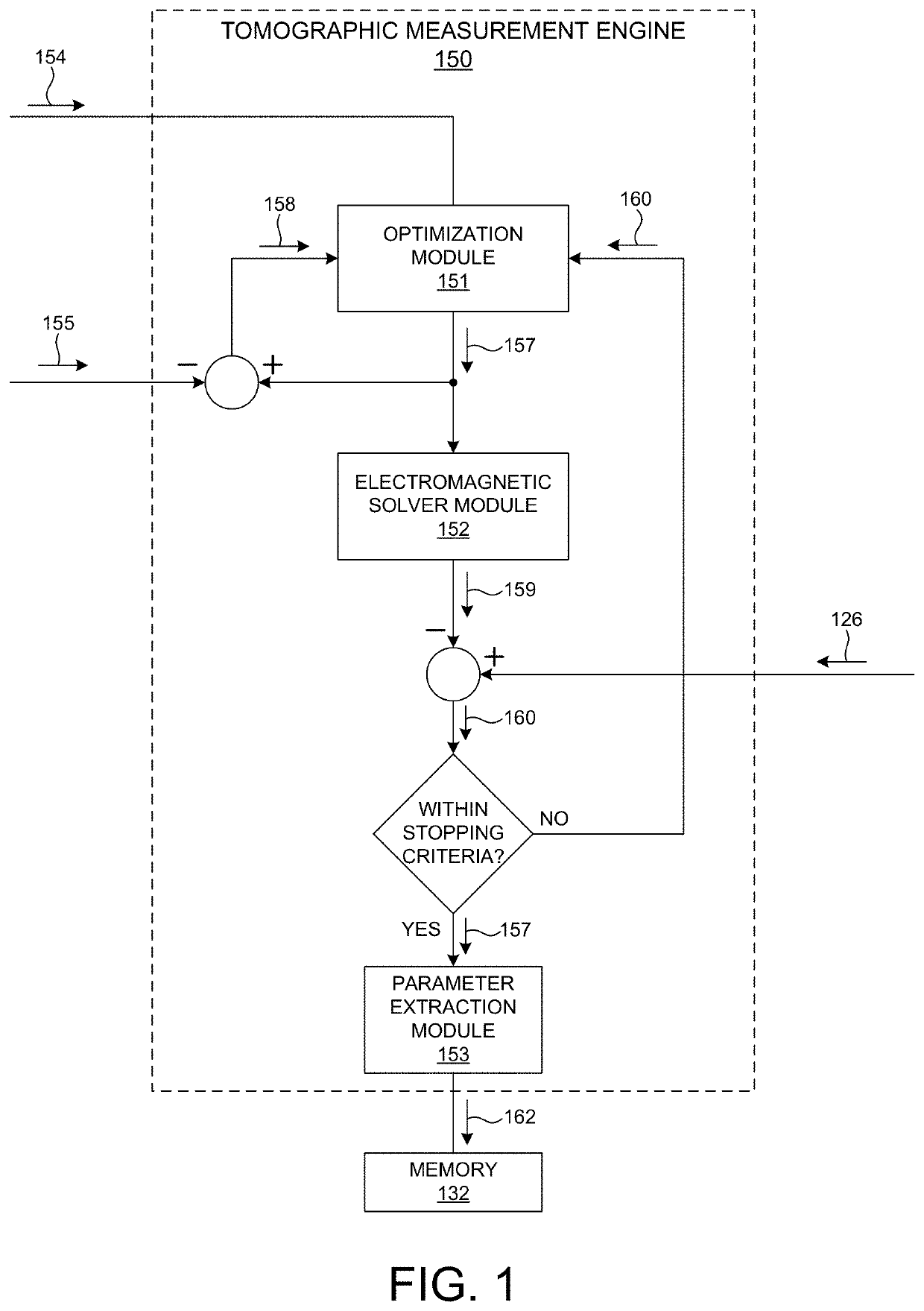
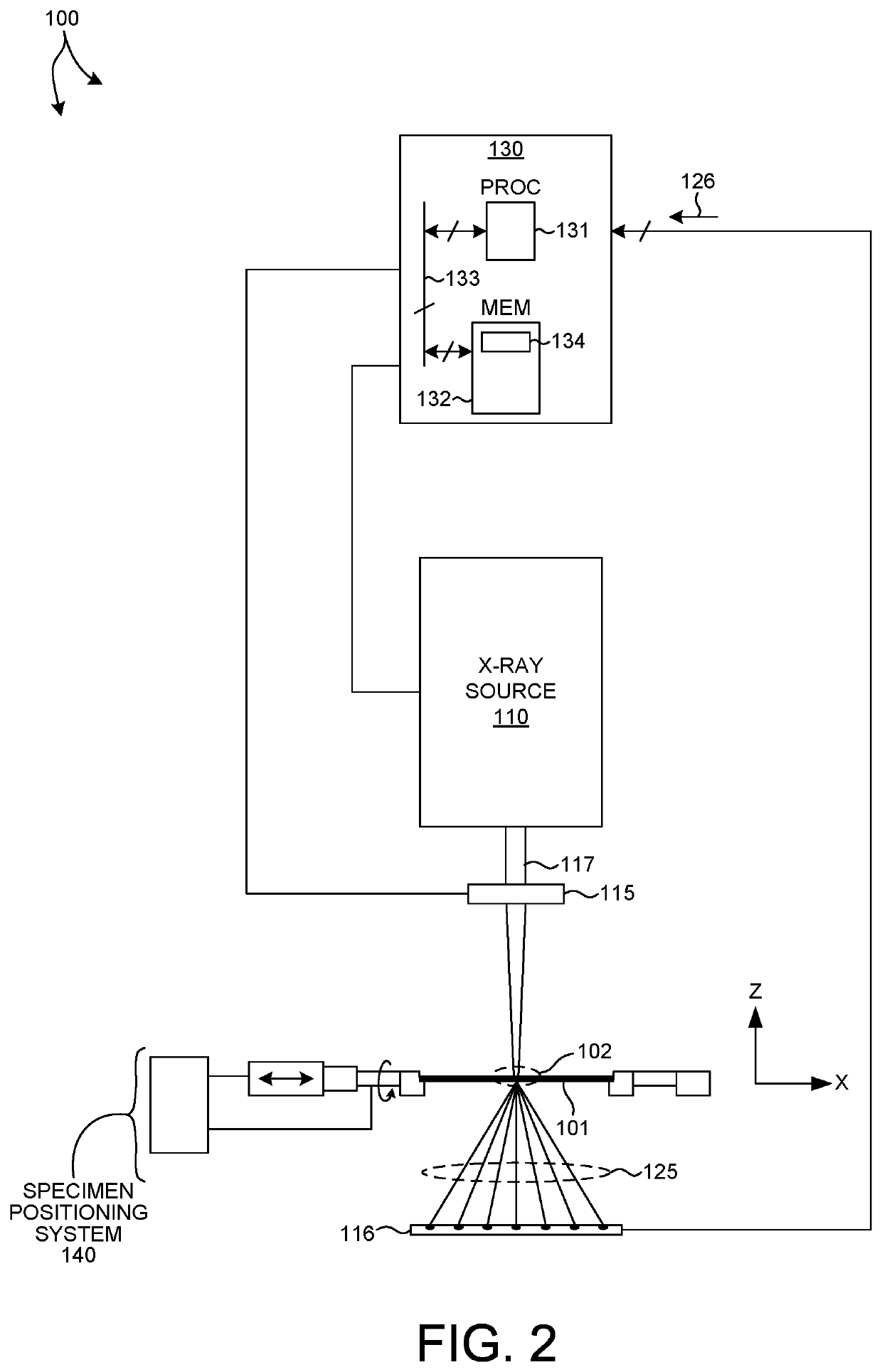
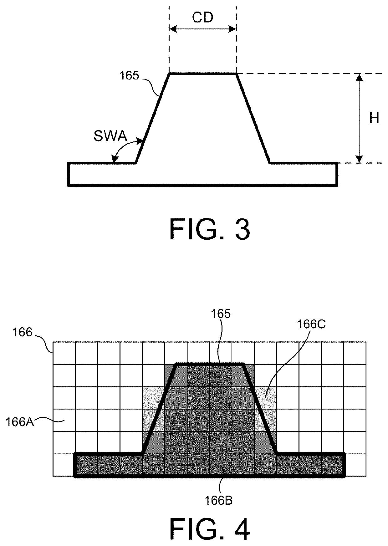
[0037]Methods and systems for improved regularization associated with tomographically resolved image based measurements of semiconductor structures are presented herein. More specifically, the regularizations described herein are based on data (e.g., simulated data, real data, or both) and parameterization of a constrained voxel model that captures known process variations. The constrained voxel model is determined based on simplified geometric models, process models, or both, characterizing the structure under measurement. Regularization based on a constrained voxel model that accurately represents process variations enables convergence to a more accurate reconstruction of the measured structure with less computational effort. This enables semiconductor measurements with reduced data acquisition requirements, e.g., f...


PUM


Abstract

Methods and systems for improved regularization associated with tomographically resolved image based measurements of semiconductor structures are presented herein. The regularizations described herein are based on measurement data and parameterization of a constrained voxel model that captures known process variations. The constrained voxel model is determined based on simplified geometric models, process models, or both, characterizing the structure under measurement. A constrained voxel model has dramatically fewer degrees of freedom compared to an unconstrained voxel model. The value associated with each voxel of the constrained voxel model depends on a relatively small number of independent variables. Selection of the independent variables is informed by knowledge of the structure and the underlying fabrication process. Regularization based on a constrained voxel model enables faster convergence and a more accurate reconstruction of the measured structure with less computational effort. This enables semiconductor measurements with reduced data acquisition requirements, and reduced measurement time.

Description

CROSS REFERENCE TO RELATED APPLICATION[0001]The present application for patent claims priority under 35 U.S.C. § 119 from U.S. provisional patent application Ser. No. 62 / 942,735 entitled “Data Driven Hybrid Tomography Using Simplified Models,” filed Dec. 2, 2019, the subject matter of which is incorporated herein by reference in its entirety.TECHNICAL FIELD[0002]The described embodiments relate to metrology systems and methods, and more particularly to methods and systems for improved measurement of semiconductor structures.BACKGROUND INFORMATION[0003]Semiconductor devices such as logic and memory devices are typically fabricated by a sequence of processing steps applied to a specimen. The various features and multiple structural levels of the semiconductor devices are formed by these processing steps. For example, lithography among others is one semiconductor fabrication process that involves generating a pattern on a semiconductor wafer. Additional examples of semiconductor fabric...

Claims


Application Information

Patent Timeline
Patent Type & Authority Applications(United States)
IPC IPC(8): G06T7/00G06T7/60G06T11/00G06N20/00
CPCG06T7/0006G06T7/60G06T2207/10116G06N20/00G06T2207/30148G06T11/008G06T11/006G06T2211/424G06N3/088G06N3/045
Inventor PANDEV, STILIAN IVANOV
Owner KLA TENCOR TECH CORP
Why Eureka
Try Eureka