
Process, reactor and system for fabrication of free-standing two-dimensional nanostructures using plasma technology

a two-dimensional nanostructure and plasma technology, applied in plasma technology, chemical/physical/physico-chemical processes, gas-gas reaction processes, etc., can solve the problems of affecting the quality of plasma products

Pending Publication Date: 2021-06-24
INST SUPERIOR TECH
View PDF0 Cites 0 Cited by
  • Summary
  • Abstract
  • Description
  • Claims
  • Application Information

AI Technical Summary

Benefits of technology

The present invention relates to a process for producing self-standing two-dimensional nanostructures by using a microwave plasma reactor. The process involves the steps of producing a stream of a mixture of inert gas and precursor, decomposing the precursor into its atomic and molecular constituents, exposing the precursor constituents to infrared radiation, and collecting the nanostructures formed by nucleation of the precursor constituents. The invention also includes a microwave plasma reactor with a hollow body, consisting of a surface wave launching part, a plasma formation transient part, and a nucleation part of precursor constituents. The reactor has three inner zones of operation that are connected sequentially. The invention also includes a cooling device for cooling the reactor body and an ultraviolet radiation source for irradiating the inner zone defined by the nucleating part of the reactor body. The technical effects of the invention include improved production of nanostructures with controlled size and shape, reduced production costs, and improved efficiency of the production process.

Problems solved by technology

However, mechanical, optical, and electrical performances of graphene crucially depend on its structural characteristics, i.e., number of mono-layers (whose growth limits the desirable quantum mechanical properties), presence of sp3 carbons, defects, etc.
However, this process leads to relatively low production rates (around 1 mg / h), when compared to the reference level for industrial applications (about 1 g / h).
These techniques present several drawbacks, such as degradation of nanostructure properties due to the interference from transition metals, the need to use expensive catalysts (Fe, Co, Cu, Ni, etc.), the very high processing temperatures, the length and complexity of production procedures, the use of hazardous chemicals and, above all, the very limited control over the assembly process of nanostructures (E. Tatarova et al, “Plasmas for Environmental Issues: From hydrogen production to 2D materials assembly” 2014 Plasma Sources Sci. Technol. 23 063002-063054).
Therefore, existing techniques are not yet capable of providing two-dimensional nanostructures with pre-defined and well controlled physicochemical and structural properties, while at the same time ensuring production rates appropriate to industrial applications.
To the previous constraints, it should be added that state of the art “bottom-up” approaches generally require the use of a substrate, consisting of a solid surface, which may limit the success of the intended applications.
However, one should emphasize that this work maintains other previously mentioned constraints, namely the low purity of the nanostructures produced, of which only some are graphene sheets constituted by two or three carbon layers (the remaining correspond to other carbon allotropes), and the low production rates achieved (about 1 mg / h).
However, these proposals have not solved other above mentioned problems, such as the low graphene production rate, of about 0.5 mg / h, and the relatively low purity level of the obtained product, which is produced with oxygen incorporated.

Method used


Image

  • Process, reactor and system for fabrication of free-standing two-dimensional nanostructures using plasma technology
  • Process, reactor and system for fabrication of free-standing two-dimensional nanostructures using plasma technology
  • Process, reactor and system for fabrication of free-standing two-dimensional nanostructures using plasma technology

Examples


examples

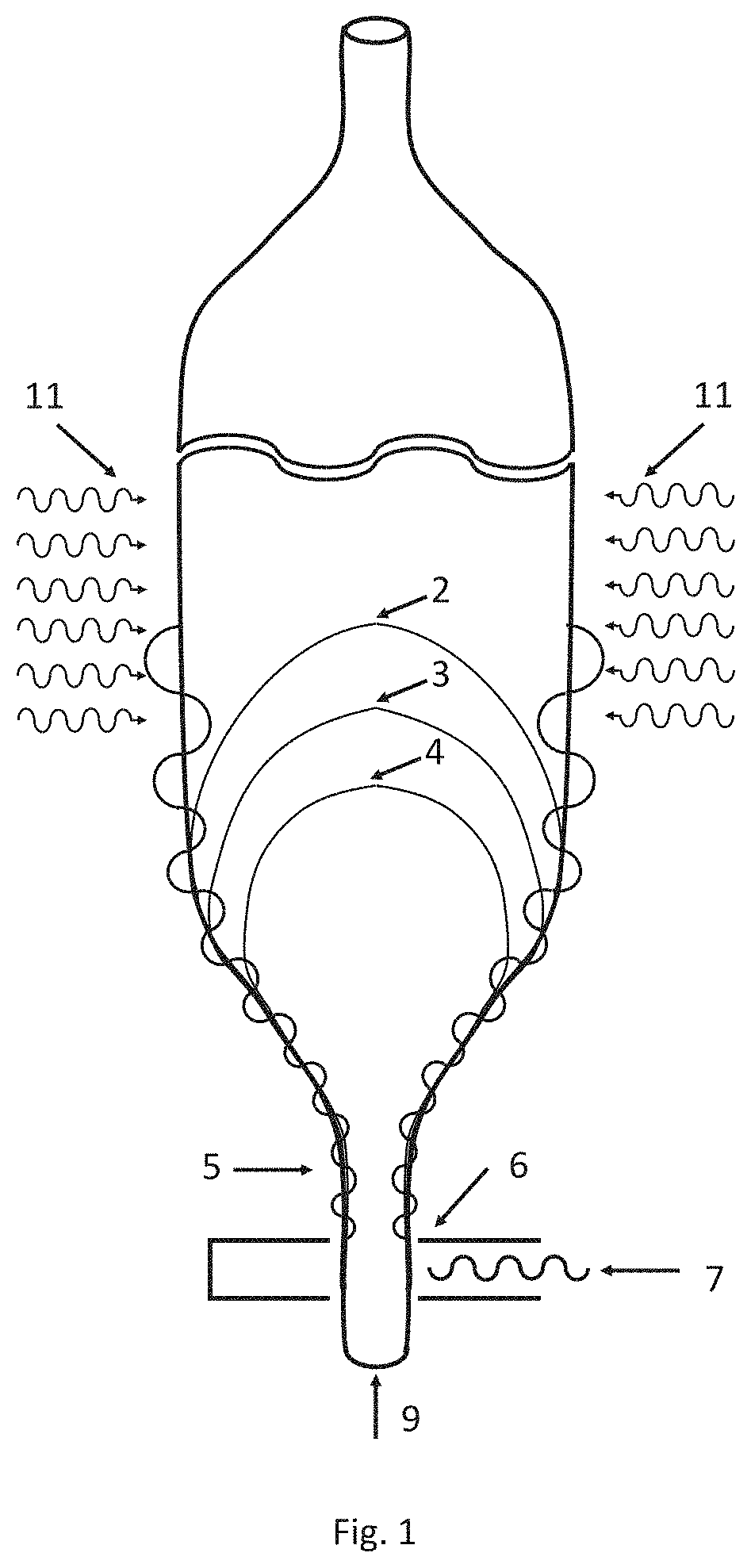
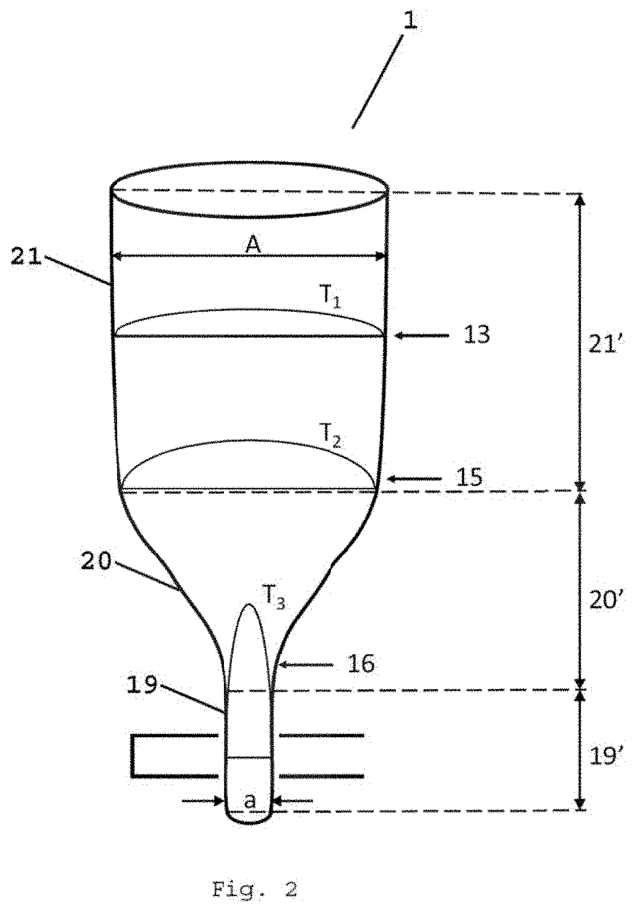
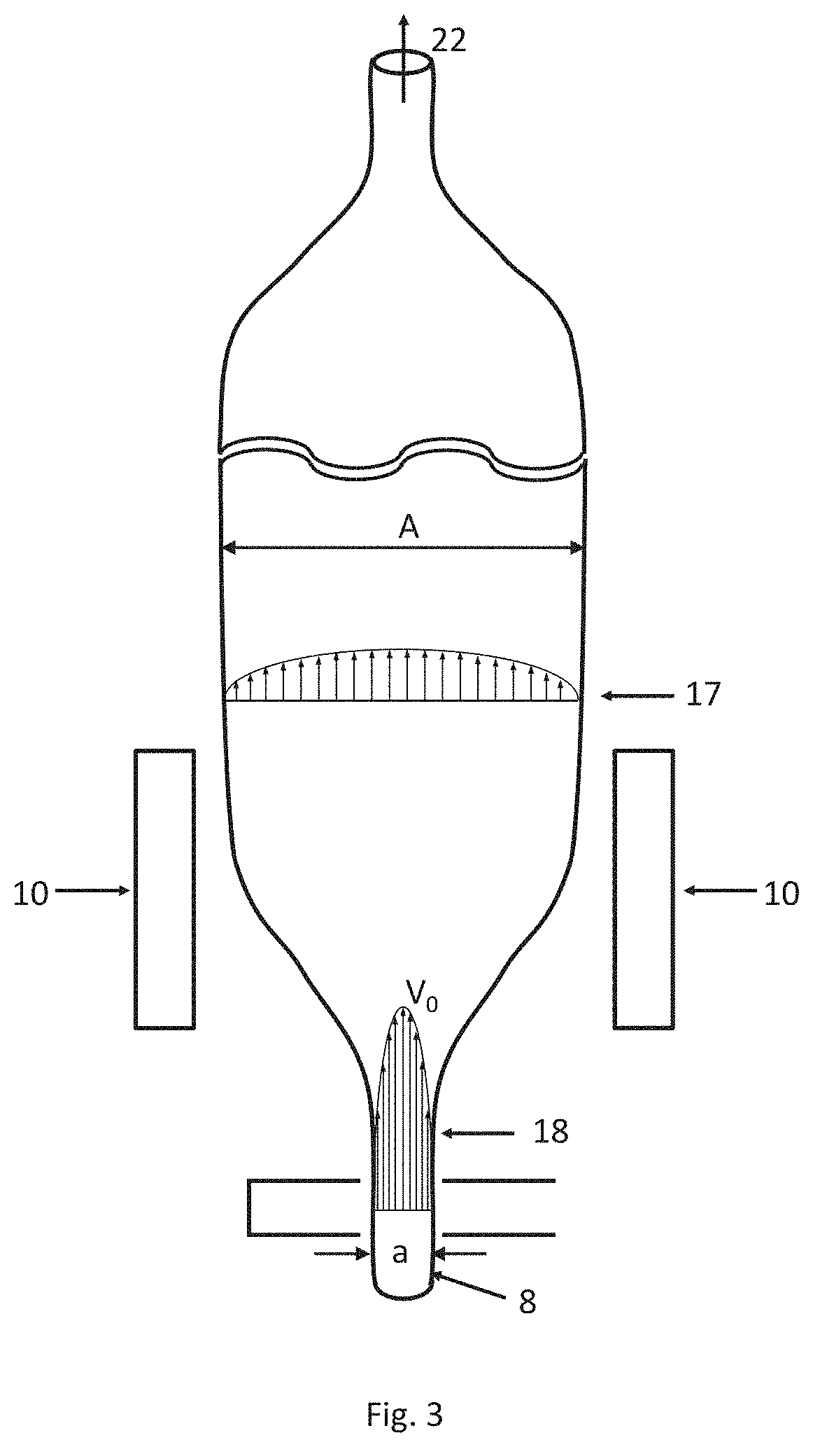
[0144]1. For the production of graphene with a production rate of more than 1 gram per hour, a plasma reactor formed by a quartz tube comprising a surface wave launching part (19) with an internal radius of 18.0 mm, a transient part (20), with an increasing internal radius, of 18.0 mm to 75.0 mm; and a nucleating part (21), with an internal radius of 75.0 mm, is used. First, a mixture composed of ethylene or acetylene as precursors, with an incorporation rate in the mixture of 8.3×10⁻⁶ m3 / s and argon as carrier gas, with a flow rate of 8.3×10⁻⁴ m3 / s, is produced. Flow rates are monitored by a controller coupled to two flow meters. Next, the said mixture formed by ethylene or acetylene and argon is introduced in stream regime (12) through a connection (14), using an injection unit (see FIG. 4), in an admission part (8) of the reactor, constituted by a quartz tube and installed in the surface wave launching part (19). Any other gas injection system capable of performing this function ...


PUM

PropertyMeasurementUnit
temperatureaaaaaaaaaa

Abstract

The present invention relates to a process, reactor and system to produce self-standing two-dimensional nanostructures, using a microwave-excited plasma environment. The process is based on injecting, into a reactor, a mixture of gases and precursors in stream regime. The stream is subjected to a surface wave electric field, excited by the use of microwave power which is introduced into a field applicator, generating high energy density plasmas, that break the precursors into its atomic and / or molecular constituents. The system comprises a plasma reactor with a surface wave launching zone, a transient zone with a progressively increasing cross-sectional area, and a nucleation zone. The plasma reactor together with an infrared radiation source provides a controlled adjustment of the spatial gradients, of the temperature and the gas stream velocity.

Description

FIELD OF THE INVENTION[0001]The present invention generally relates to a process and to a reactor and system for the selective fabrication of free-standing two-dimensional nanostructures using plasma technology, in particular microwave plasma.BACKGROUND OF THE INVENTION[0002]Currently, the development of new two-dimensional nanostructures is considered one of the science and technology research areas that presents greater demand and, as such, with greater strategic value.[0003]Graphene is the most eminent example of a two-dimensional (carbon-based) nanostructure with an increasing demand, as it possesses many extraordinary properties, with potential applications in numerous scientific and engineering disciplines.[0004]However, mechanical, optical, and electrical performances of graphene crucially depend on its structural characteristics, i.e., number of mono-layers (whose growth limits the desirable quantum mechanical properties), presence of sp3 carbons, defects, etc.[0005]Currentl...

Claims


Application Information

Patent Timeline
Patent Type & Authority Applications(United States)
IPC IPC(8): C01B32/184B01J12/00H05H1/46
CPCC01B32/184B82Y30/00H05H1/46B01J12/002B82Y40/00C01B32/186H05H1/4615C01P2004/20C01P2004/64B01J2219/0898B01J19/126B01J2219/1224B01J2219/1206
Inventor TATAROVA, ELANA STEFANOVADOS SANTOS DUARTE VIEIRA HENRIQUES, JULIO PAULODA MOTA CAPITAO LEMOS ALVES, LUIS PAULOSOARES GONCALVES, BRUNO MIQUEL
Owner INST SUPERIOR TECH
Learn More