Electrophoretic display layer with thin film top electrode
a technology of electrophoretic display and top electrode, applied in non-linear optics, instruments, optics, etc., can solve the problems of adhesive layer failure, image pixel mixing together, and the standard method of front plane laminate production has some limitations, so as to prevent moisture ingress, reduce the amount of energy, and high local electric field
- Summary
- Abstract
- Description
- Claims
- Application Information
AI Technical Summary
Benefits of technology
Problems solved by technology
Method used
Image
Examples
example 1
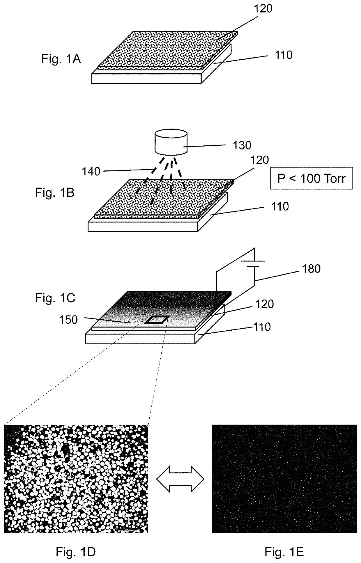
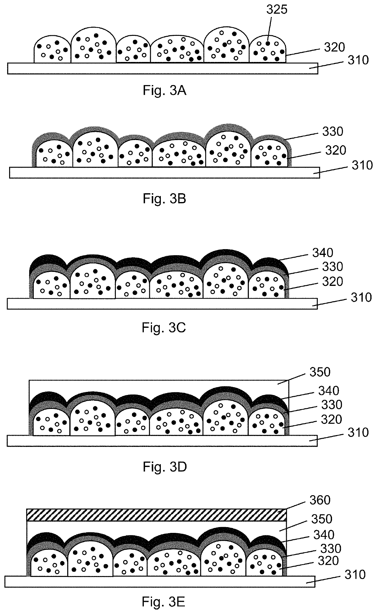
[0063]A layer of encapsulated electrophoretic media was produced by slot die coating a polyurethane slurry of collagen / acacia capsules of black and white charged electrophoretic media onto a PET-ITO substrate, as illustrated in FIG. 4A. More details of the encapsulation process, the slurry formation, and the slot coating process can be found in U.S. Pat. No. 6,982,178. Prior to coating, Kapton® tape was used to mask the edges of the substrate, thereby allowing for an easy electrical connection at the completion of the process. After curing the binder with heat, a conformal coating of 100 nm of Indium Tin Oxide (ITO) was deposited onto a monolayer of capsules using radio-frequency sputtering (Semicore Equipment, Livermore, Calif.). During the sputtering process, the layer of encapsulated electrophoretic media was exposed to 8 mTorr of vacuum for 1500 seconds.
[0064]An electrophoretic display was created by proving an electrical potential between the sputtered ITO electrode and the ITO...
example 2
[0066]A second sample was prepared as in EXAMPLE 1, but additionally included a polyurethane planarization layer atop the sputtered 100 nm ITO, and a film of matte PET was laminated on top of the planarization layer for additional protection. The white state of the second sample remained almost the same while the dark state was reduced by 36% to 29L*.
TABLE 1Reflective electro-optic measurements for samples driven at ±30V.White StateDark(L*)State (L*)Contrast RatioSample 1: Viewed from75.7019.03.98PET ITO sideSample 1: Viewed from80.245.41.76sputtered ITO sideSample 2: Viewed from79.9729.32.73sputter ITO side(with planarization layer andprotective sheet)
[0067]It is likely that the improved dark state with the planarization layer and matte PET film was an artifact of the measurement technique. Because the sputtered ITO is very smooth, it reflects a good amount of the incident light, even when the electrophoretic medium has been driven to a dark state. Once the matte PET top protective...
example 3
[0068]Another variation on Example 1 was created, which included a thin (10 nm thick) layer of SiO2 deposited via RF sputtering directly atop the slot-coated microcapsules, which was in turn followed with 100 nm of Indium Tin Oxide (ITO), also deposited using radio-frequency sputtering. The resulting assembly is similar to FIG. 5C, described above.
[0069]Adding an intervening dielectric layer greatly improved the measured kickback, especially at higher temperatures, as shown in FIG. 8. The kickback manifests itself as optical self-erasing; when an electro-optic display is driven from one extreme optical state to the opposed extreme optical state by application of a drive pulse and then allowed to stand with no electric field applied to the electro-optic medium, for a short time, the electro-optic medium relaxes back towards the one extreme optical state from which it was driven. See, e.g., FIG. 7. Notably, as shown in FIG. 8, the kickback was approximately half as large in the presen...
PUM
 Abstract
Description
Claims
Application Information


