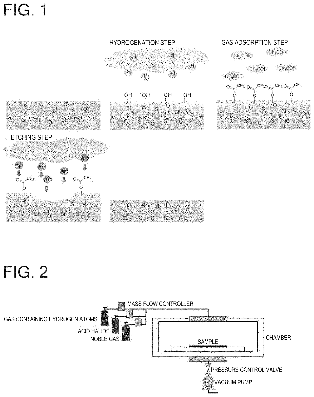
Atomic layer etching using acid halide
a technology of atomic layer and acid halide, which is applied in the direction of basic electric elements, electrical equipment, chemical instruments and processes, etc., can solve the problems of high accuracy required in each step of etching, difficulty in adjusting the thickness of the modified layer to the thickness of a single atomic layer, and conventional etching techniques and film forming techniques have already faced such difficulties in handling such requirements, so as to achieve better controllability and reproducibility
- Summary
- Abstract
- Description
- Claims
- Application Information
AI Technical Summary
Benefits of technology
Problems solved by technology
Method used
Image

Examples
example 1
[0065]In accordance with the conditions of Table 1, a SiO2 sample (SiO2: 1,000 nm on Si substrate) and polysilicon (Poly-Si) samples (Poly-Si: 300 nm on SiO2 substrate; 100 nm on Si substrate) were subjected to 30 cycles of etching while using H2 as a gas containing hydrogen atoms in the hydrogenation step, CF3COF as an acid halide in the acid halide adsorption step, and using Ar as a noble gas and setting RF power to 60 W in the etching step. One cycle progresses in the order of (1)→(2)→(3)→(4)→(5)→(6) of Table 1, and processing is started from (1) again in the next cycle. As a result, the etched amount of SiO2 was 9.3 nm (0.31 nm / cycle) and the etched amount of Poly-Si was 0.0 nm (0.0 nm / cycle).
[0066]Next, when the same samples were subjected to 60 cycles of etching under the same conditions, the etched amount of SiO2 was 14.6 nm (0.24 nm / cycle) and the etched amount of Poly-Si was 0.0 nm (0.0 nm / cycle).
[0067]Further, after 90 cycles of etching, the etched amount of SiO2 was 19.9 ...
example 2
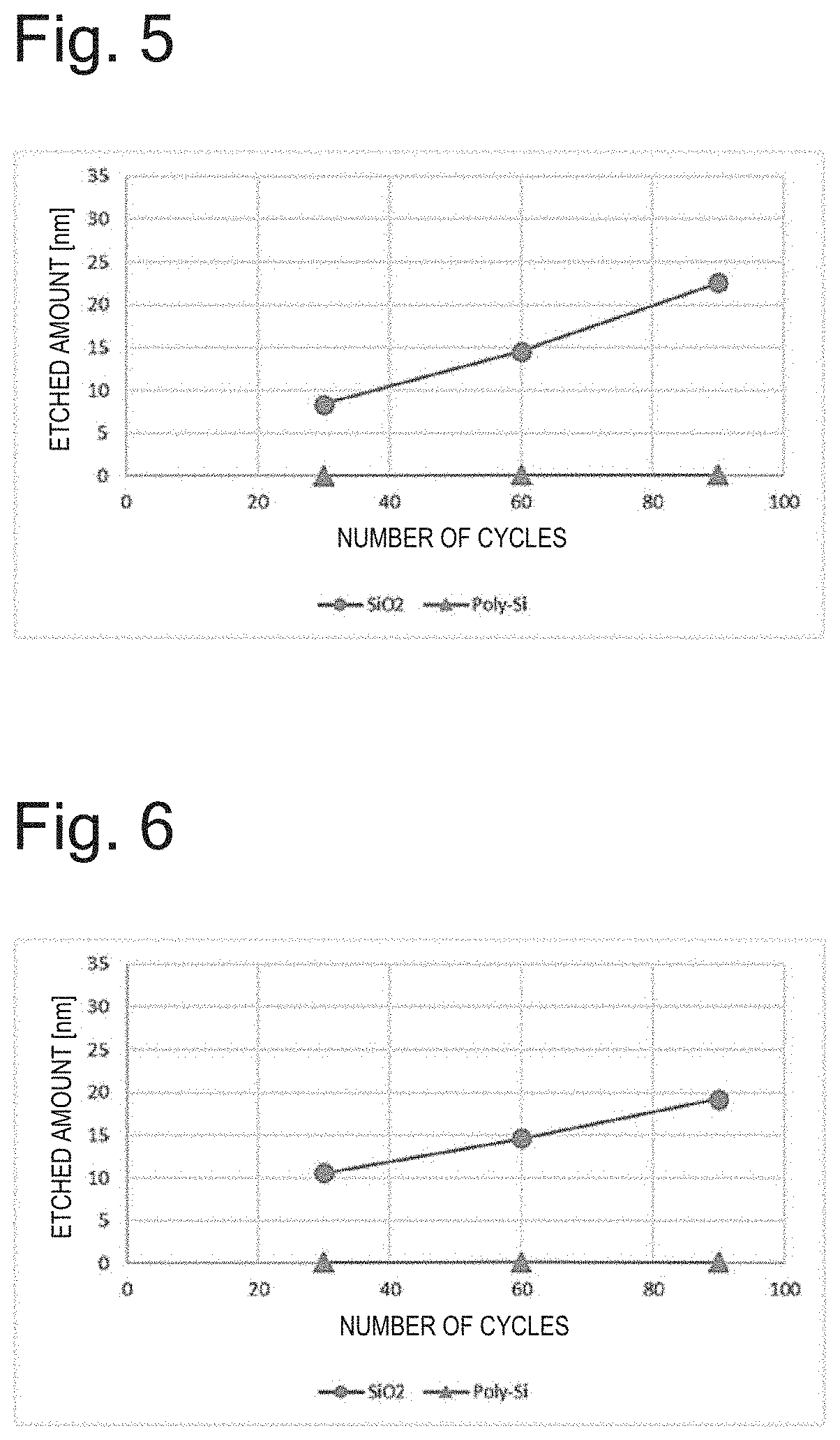
[0069]In accordance with the conditions of Table 1, a SiO2 sample (SiO2: 1,000 nm on Si substrate) and Poly-Si samples (Poly-Si: 300 nm on SiO2 substrate; 100 nm on Si substrate) were subjected to 30 cycles of etching while using H2 as a gas containing hydrogen atoms in the hydrogenation step, CHF2COF as an acid halide in the acid halide adsorption step, and using Ar as a noble gas and setting RF power to 60 W in the etching step. As a result, the etched amount of SiO2 was 11.5 nm (0.38 nm / cycle) and the etched amount of Poly-Si was 0.2 nm (0.007 nm / cycle).
[0070]Next, when the same samples were subjected to 60 cycles of etching under the same conditions, the etched amount of SiO2 was 19.1 nm (0.32 nm / cycle) and the etched amount of Poly-Si was 0.1 nm (0.002 nm / cycle).
[0071]Further, after 90 cycles of etching, the etched amount of SiO2 was 31.4 nm (0.35 nm / cycle) and the etched amount of Poly-Si was 0.4 nm (0.004 nm / cycle).
[0072]The above results are summarized in FIG. 4.
example 3
[0073]In accordance with the conditions of Table 1, a SiO2 sample (SiO2: 1,000 nm on Si substrate) and Poly-Si samples (Poly-Si: 300 nm on SiO2 substrate; 100 nm on Si substrate) were subjected to 30 cycles of etching while using H2 as a gas containing hydrogen atoms in the hydrogenation step, CF3COF as an acid halide in the acid halide adsorption step, and using Ar as a noble gas and setting RF power to 30 W in the etching step. As a result, the etched amount of SiO2 was 8.4 nm (0.28 nm / cycle) and the etched amount of Poly-Si was 0.0 nm (0 nm / cycle).
[0074]Next, when the same samples were subjected to 60 cycles of etching under the same conditions, the etched amount of SiO2 was 14.6 nm (0.24 nm / cycle) and the etched amount of Poly-Si was 0.0 nm (0 nm / cycle).
[0075]Further, after 90 cycles of etching, the etched amount of SiO2 was 22.6 nm (0.25 nm / cycle) and the etched amount of Poly-Si was 0.1 nm (0.001 nm / cycle).
[0076]The above results are summarized in FIG. 5.
PUM
 Abstract
Description
Claims
Application Information