
Carrier-containing metal foil and method for manufacturing millimeter-wave antenna substrate using same

Active Publication Date: 2021-10-21
MITSUI MINING & SMELTING CO LTD
View PDF1 Cites 0 Cited by
  • Summary
  • Abstract
  • Description
  • Claims
  • Application Information

AI Technical Summary

Benefits of technology

The patent is about improving the manufacturing of semiconductor packages, specifically millimeter-wave antenna substrates, using a technique called Au plating. By controlling the thickness of a layer that helps release the carrier, a metal layer mainly composed of Au or Pt, and a reduction in transmission loss and resistance, the carrier-attached metal foil provided in this patent has excellent properties for use in semiconductor packages. Overall, this invention aims to provide a better material for manufacturing millimeter-wave antenna substrates.

Problems solved by technology

In this regard, when a millimeter-wave antenna substrate or the like is produced using a conventional career-attached copper foil, the chemical stability of Cu is low, which may disadvantageously cause high resistance (for example, interconnection resistance with Au plating).
In the manufacture of the millimeter-wave antenna substrate and the like, a resin (for example, a thickness of 200 μm or more) which is comparatively thick as an insulating layer is laminated on the carrier-attached metal foil to reduce interference, so that the carrier-attached metal foil is apt to be subjected to a stress from the resin, which may cause unstable release of the career.

Method used


Image

  • Carrier-containing metal foil and method for manufacturing millimeter-wave antenna substrate using same
  • Carrier-containing metal foil and method for manufacturing millimeter-wave antenna substrate using same
  • Carrier-containing metal foil and method for manufacturing millimeter-wave antenna substrate using same

Examples


example 1

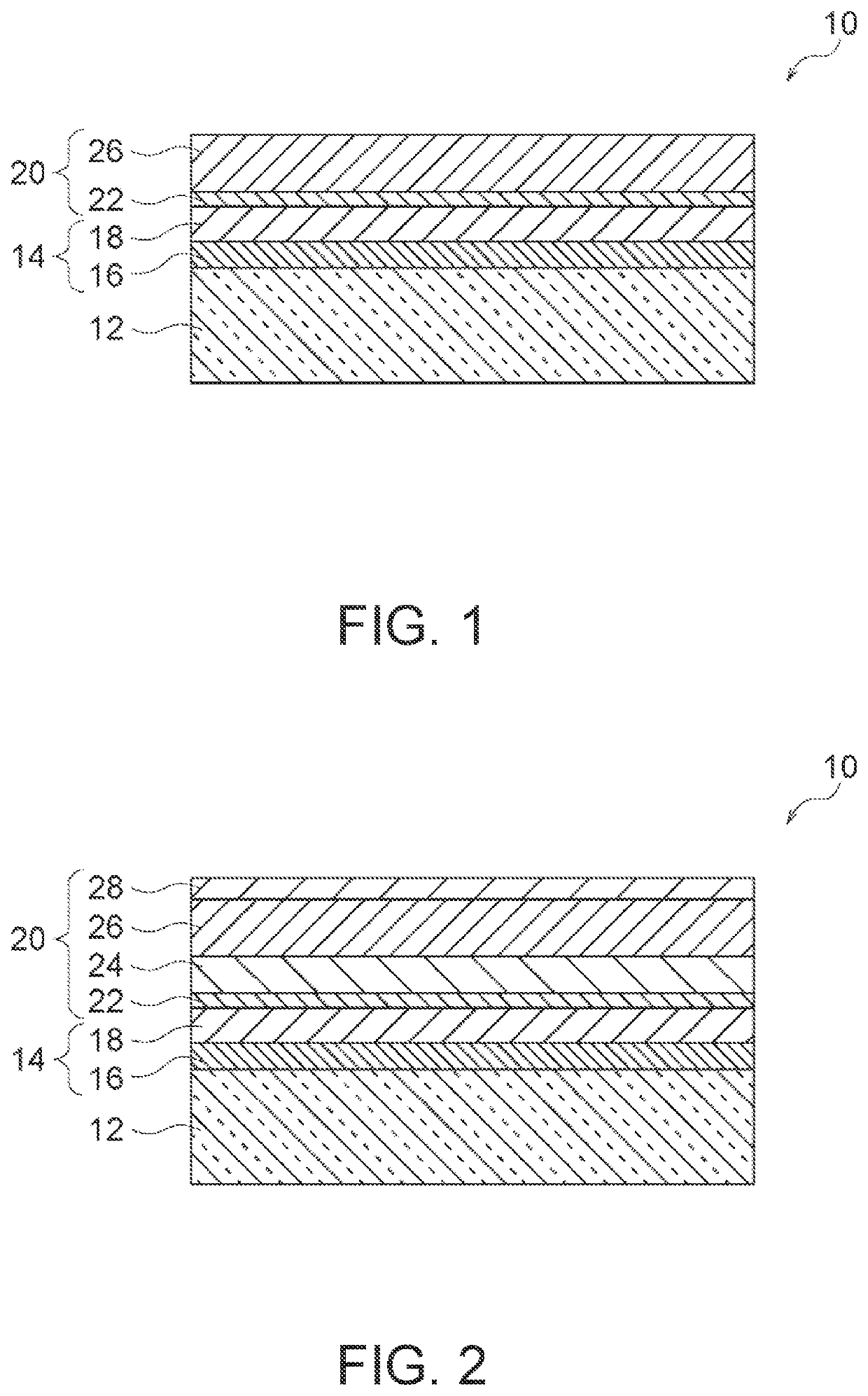
[0065]On a career 12, an adhesion layer 16, a release assistance layer 18, a carbon layer 22, a second metal layer 24, and a first metal layer 26 were deposited in this order, to manufacture a carrier-attached metal foil 10. Specific procedures will be described below.

(1) Preparation of Career

[0066]A glass sheet having a thickness of 1.1 mm (material: soda-lime glass, arithmetic average roughness Ra: 0.6 nm) was prepared as the career 12.

(2) Formation of Adhesion Layer

[0067]On the career 12, a titanium layer a thickness of 50 nm was formed as the adhesion layer 16 by a sputtering method. The sputtering was performed under the following conditions using the following apparatus.[0068]Apparatus: single wafer type magnetron sputtering apparatus (MLS 464, manufactured by Canon Tokki Corporation)[0069]Target: titanium target (purity: 99.999%) having a diameter of 8 inches (203.2 mm)[0070]Ultimate vacuum: less than 1×10⁻⁴ Pa[0071]Sputtering pressure: 0.35 Pa[0072]Sputtering power: 1000 W (...

example 2

[0105]A carrier-attached metal foil was produced in the same manner as in Example 1 except that the first metal layer 26 was formed in the above (6), and a barrier layer 28 was then formed as follows.

(7) Formation of Barrier Layer

[0106]A nickel layer having a thickness of 30 nm was formed as the barrier layer on the surface of the first metal layer 26 on the opposite side of the second metal layer 24 by a sputtering method. The sputtering was performed under the following conditions using the following apparatus.[0107]Apparatus: single wafer type DC sputtering apparatus (MLS 464, manufactured by Canon Tokki Corporation)[0108]Target: nickel target (purity: 99.9%) having a diameter of 8 inches (203.2 mm)[0109]Carrier gas: argon gas (flow rate: 100 sccm)[0110]Ultimate vacuum: less than 1×10⁻⁴ Pa[0111]Sputtering pressure: 0.35 Pa[0112]Sputtering power: 1000 W (3.1 W / cm2)

example 3 (

Comparison)

[0113]A carrier-attached metal foil was produced in the same manner as in Example 1 except that a sputtering copper target (purity: 99.98%) was used to form a copper layer as the first metal layer 26 in place of the Au layer.


PUM

PropertyMeasurementUnit
Thicknessaaaaaaaaaa
Thicknessaaaaaaaaaa
Thicknessaaaaaaaaaa

Abstract

Provided is a carrier-attached metal foil which has excellent carrier-releasability and excellent selective metal layer-etchability, and can achieve a reduction in transmission loss and resistance in a semiconductor package (for example, a millimeter-wave antenna substrate) manufactured using the same. The carrier-attached metal foil includes: (a) a carrier; (b) a release functional layer on the carrier and including (b1) an adhesion layer disposed closer to the carrier and having a thickness of more than 10 nm and less than 200 nm and (b2) a release assistance layer disposed farther from the carrier and having a thickness of 50 nm or more and 500 nm or less; and (c) a composite metal layer on the release functional layer and including (c1) a carbon layer disposed closer to the release assistance layer, and (c2) a first metal layer disposed farther from the release assistance layer and mainly composed of Au or Pt.

Description

TECHNICAL FIELD[0001]The present invention relates to a carrier-attached metal foil and a method for manufacturing a millimeter-wave antenna substrate using the same.BACKGROUND ART[0002]In recent years, multilayering of printed wiring boards has gradually prevailed to provide an increased mounting density of the printed wiring board to provide a decreased size thereof. Such multilayer printed wiring boards have been used for reductions in weight and size of many portable electronic devices. A further reduction in the thickness of an interlayer insulating layer and a further reduction in the weight of the wiring board are required for the multilayer printed wiring boards.[0003]As a technique for meeting such requirements, a method for manufacturing a multilayer printed wiring board using a coreless build-up method has been employed. The coreless build-up method alternately laminates (builds up) insulating layers and wiring layers without using a so-called core substrate into a multil...

Claims


Application Information

Patent Timeline
IPC IPC(8): H01Q1/22H01Q1/42H05K1/09B32B15/04
CPCH01Q1/2283B32B15/04H05K1/09H01Q1/422H01P3/082H05K2201/0355H05K3/025B32B7/06
Inventor KOMIYA, MIKIKOYANAI, TAKENORIISHII, RINTAROMATSUURA, YOSHINORI
Owner MITSUI MINING & SMELTING CO LTD
Learn More