
Semiconductor device manufacturing method

Pending Publication Date: 2021-12-23
JIANGSU LEUVEN INSTR CO LTD
View PDF0 Cites 0 Cited by
  • Summary
  • Abstract
  • Description
  • Claims
  • Application Information

AI Technical Summary

Benefits of technology

The present invention utilizes a combination of ion beam etching and reactive ion etching to effectively reduce sidewall metal contamination and structural damage, improve etching efficiency, and reduce the risk of over etching. This results in improved device performance and yield.

Problems solved by technology

As the feature size of semiconductor devices is further reduced, the conventional flash memory technology will reach its size limit.
It is relatively difficult for the material of the MTJ to produce volatile products as compared with a dry etching material such as Fe, Co, or Mg; and further an etchant gas (for example, Cl2) cannot be used, or otherwise the performance of the MTJ is degraded.
Therefore, MTJ patterning can be realized by necessarily using a relatively complicated etching method, and an etching process is very difficult and challenging.
On one hand, one implementation principle of the IBE is the use of a high physical bombardment force, but an excessively large physical bombardment force may cause disturbance in the ordering of atomic layers of the MTJ sidewall, especially in the isolation layer and the nearby core layer, thus disrupting the magnetic characteristics of the MTJ.
On the other hand, IBE is realized necessarily by using a certain angle, which brings limitations to the IBE.
As MTJ devices are made increasingly smaller in size, IBE cannot be performed to the bottom of the MTJ at a frequently used angle, thus failing to meet the requirements for separation of the MTJ devices, and making the patterning fail.
Moreover, an IBE time is relatively long, causing a limited yield of each apparatus.

Method used


Image

  • Semiconductor device manufacturing method
  • Semiconductor device manufacturing method
  • Semiconductor device manufacturing method

Examples


Embodiment Construction

[0025]To make the objective, technical solutions, and advantages of the present invention clearer, the technical solutions in the embodiments of the present invention are clearly and completely described below with reference to the accompanying drawings in the embodiments of the present invention. It should be noted that, the specific embodiments described herein are merely used for explaining the present invention, rather than limiting the present invention. The described embodiments are some rather than all of the embodiments of the present invention. Based on the described embodiments of the present invention, other embodiments acquired by those of ordinary skill in the art without creative effort all belong to the protection scope of the present invention.

[0026]In the description of the present invention, it should be noted that, the orientation or positional relationship indicated by the terms “upper”, “lower”, “steep”, “tilted”, etc. are based on the orientation or positional ...


PUM

PropertyMeasurementUnit
Thicknessaaaaaaaaaa
Thicknessaaaaaaaaaa
Dielectric polarization enthalpyaaaaaaaaaa

Abstract

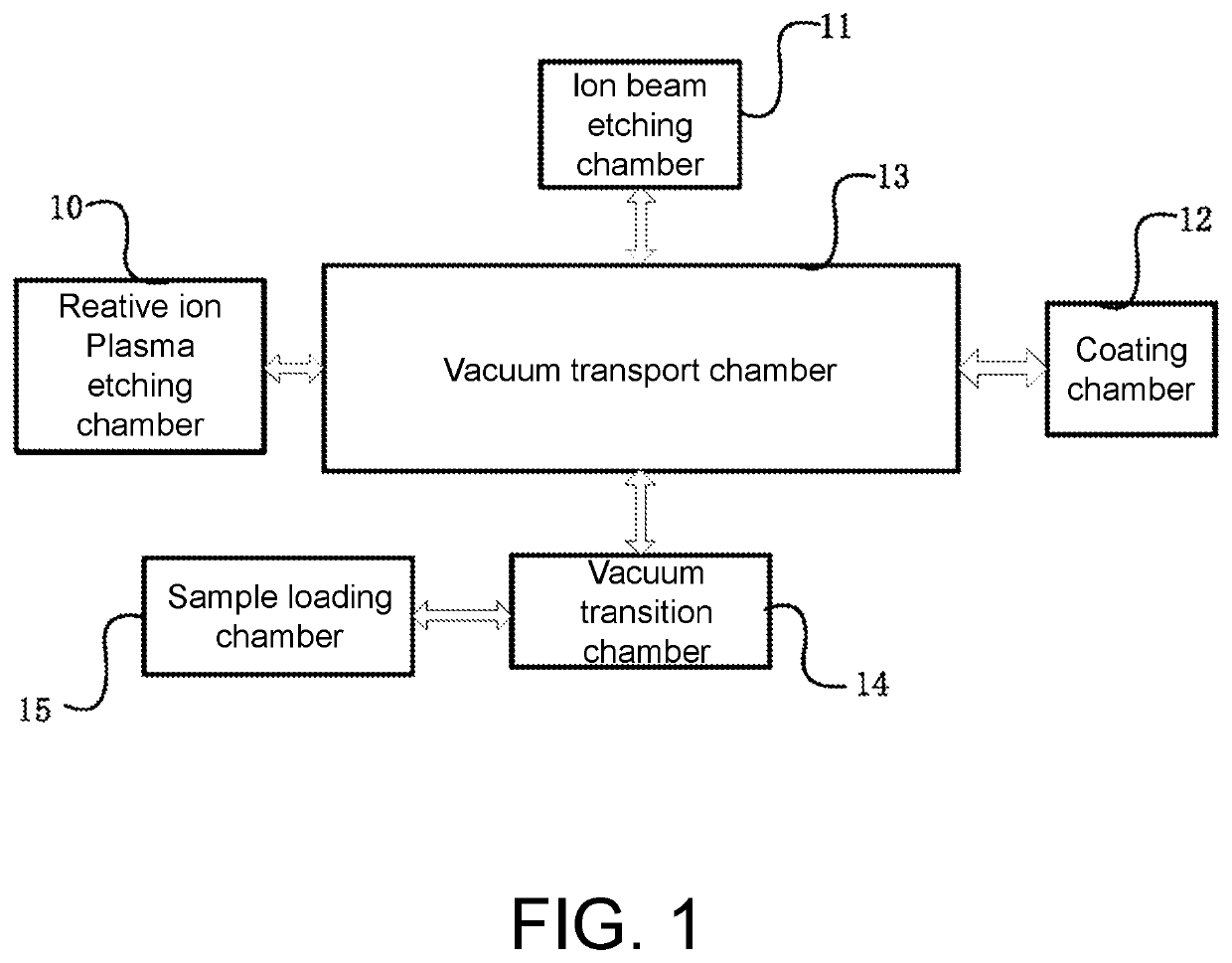
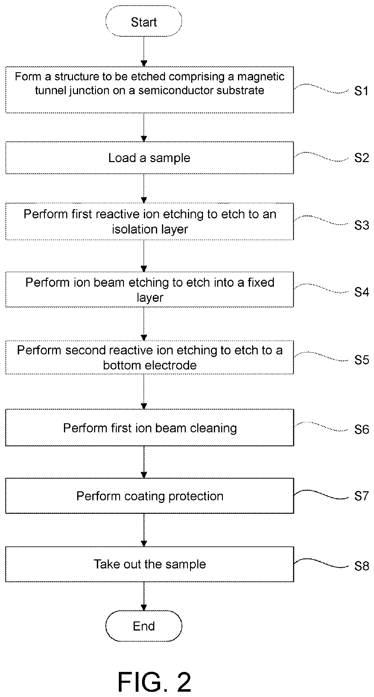
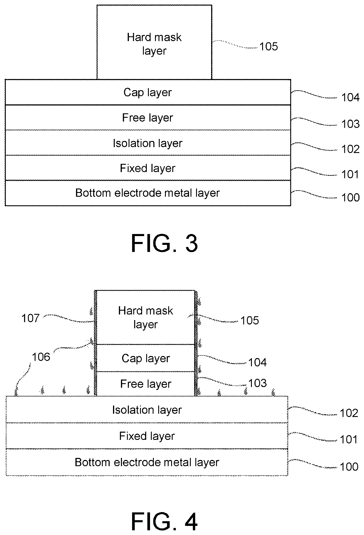
A semiconductor device manufacturing method, wherein the etching apparatus used includes a sample loading chamber (15), a vacuum transition chamber (14), a reactive ion plasma etching chamber (10), an ion beam etching chamber (11), a film coating chamber (12), and a vacuum transport chamber (13). Without interrupting the vacuum, reactive ion etching is first adopted to etch to an isolation layer (102); then, ion beam etching is performed to etch into a fixed layer (101) and stopped near a bottom electrode metal layer (100), leaving only a small amount of the fixed layer (101); subsequently, reactive ion etching is adopted to etch to the bottom electrode metal layer (100); and finally, ion beam cleaning is performed to remove metal residues and sample surface treatment, and coating protection is performed.

Description

BACKGROUNDTechnical Field[0001]The present invention relates to the field of semiconductors, and in particular, to a semiconductor device manufacturing method.Description of Related Art[0002]As the feature size of semiconductor devices is further reduced, the conventional flash memory technology will reach its size limit. In order to further improve the device performance, research and development personnel begin to actively explore new structures, new materials, and new processes. In recent years, various types of novel non-volatile memories have developed rapidly. Among these memories, an MRAM has a high-speed read / write capability of a static random access memory (SRAM), high integration of a dynamic random access memory (DRAM), and power consumption far lower than that of the DRAM; and its performance does not degrade with the use time as compared with a flash memory (Flash). Due to these advantages, the MRAM gets more and more attention from the industry and is regarded as one ...

Claims


Application Information

Patent Timeline
IPC IPC(8): H01L43/12
CPCH01L43/12H01L43/02H10N50/01C23F4/00Y02P70/50H10N50/10H10N50/80
Inventor JIANG, ZHONGYUANLIU, ZIMINGWANG, JUEBINCHE, DONGCHENCUI, HUSHANHU, DONGDONGCHEN, LUREN, HUIQUNZOU, ZHIWENXU, KAIDONG
Owner JIANGSU LEUVEN INSTR CO LTD
Learn More