

Method and apparatus for analysis of interface state of mis-hemt device
a technology of interface state and analysis method, which is applied in the field of interface state analysis methods and apparatus of metalinsulatorsemiconductor high-electron-mobility transistors, can solve the problems of difficult to guarantee the calculation result, the inability to guarantee the accuracy of the density of the interface state density, and the manufacturing of trench-gate enhancement devices
- Summary
- Abstract
- Description
- Claims
- Application Information
AI Technical Summary
Benefits of technology
Problems solved by technology
Method used
Image

Examples
first embodiment
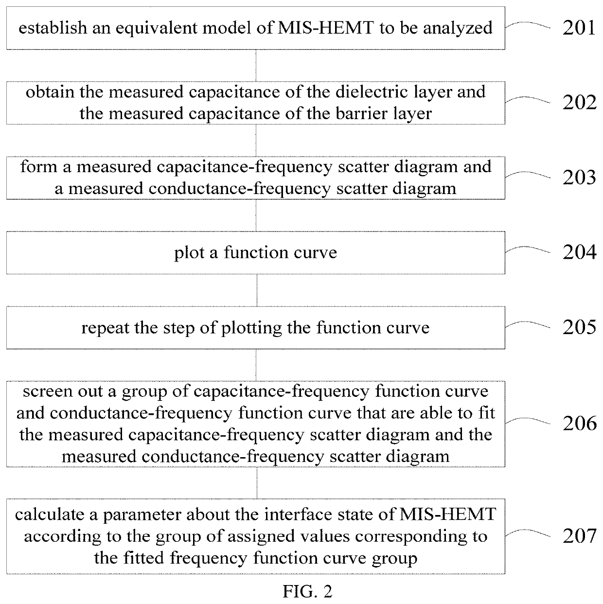
[0041]FIG. 2 schematically shows a flow chart of interface state analysis method of MIS-HEMT(s) according to this embodiment. Please refer to FIG. 2, the interface state analysis method of MIS-HEMT(s) provided herein may include the following.
[0042]Step 201: establishing an equivalent model of a MIS-HEMT device to be analyzed.
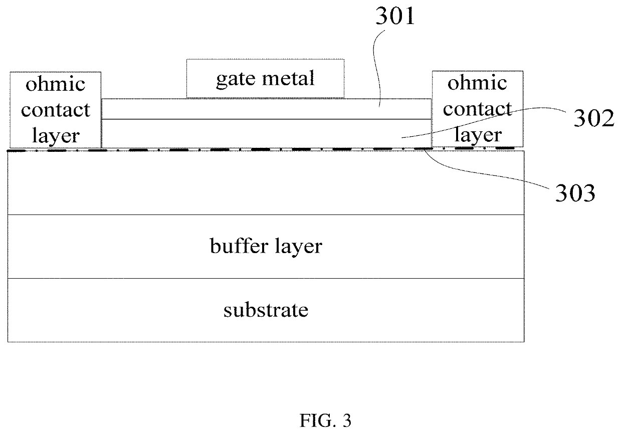
[0043]Referring to FIG. 3, the MIS-HEMT device may include a dielectric layer 301, a barrier layer 302 and a channel layer 303. It shall be noted that in the MIS-HEMT device, the material of the dielectric layer 301 is SiN, the material of the barrier layer 302 is AlGaN material, and a GaN layer is below the barrier layer 302. The GaN layer generally may be called the channel layer, but actually a channel layer may be a two-dimensional electron gas (2DEG) layer generated between the GaN layer and the barrier layer 302. Accordingly, the channel layer 303 in this embodiment refers to the 2DEG layer between the barrier layer 302 and the GaN layer.
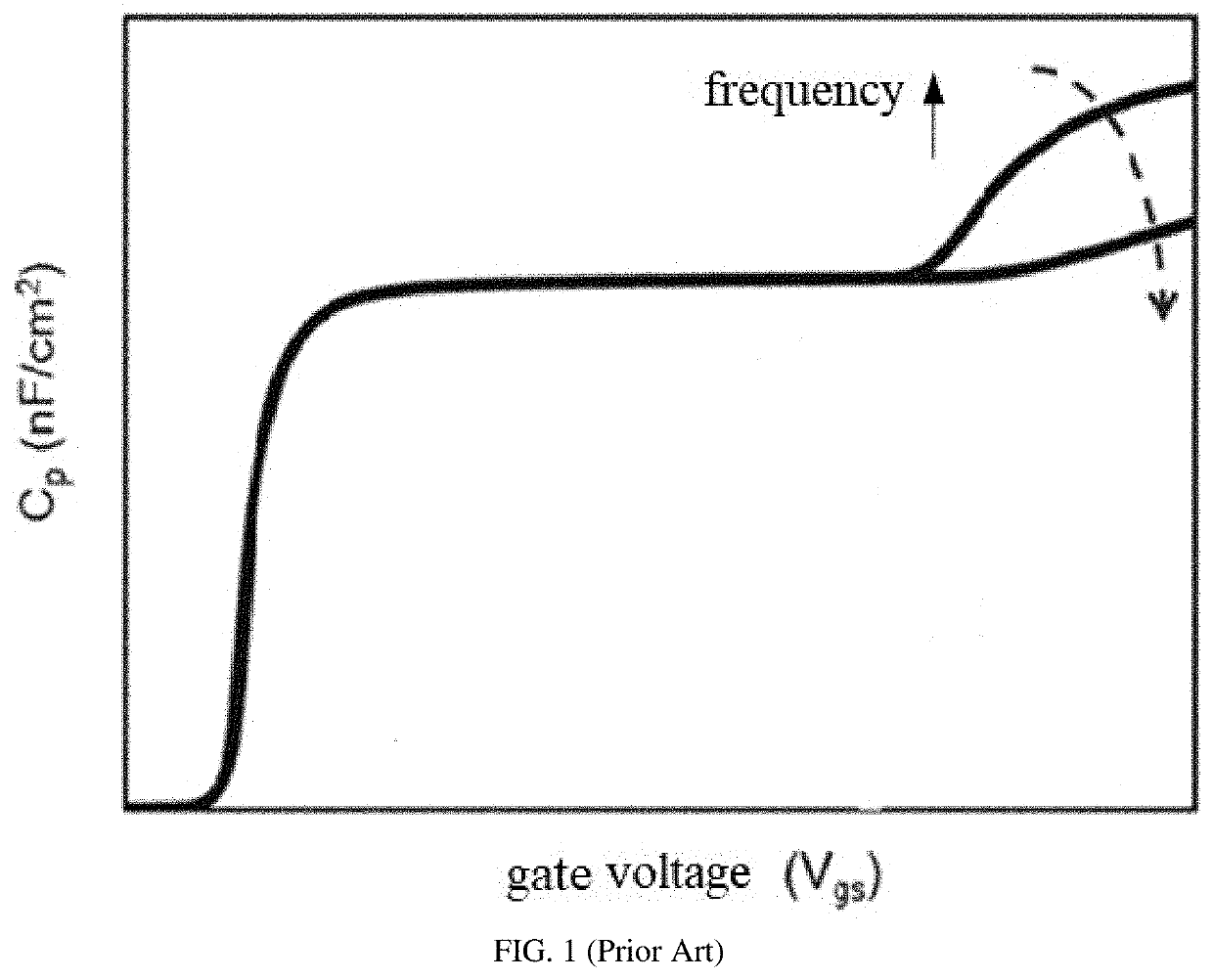
[0044]The interfa...
second embodiment
[0086]An interface state analysis apparatus of a MIS-HEMT device provided in the present embodiment may include:
[0087]a model establishing unit, configured for establishing an equivalent model of the MIS-HEMT device to be analyzed, wherein the MIS-HEMT device may include a dielectric layer, a barrier layer and a channel layer; the equivalent model may include a dielectric-layer equivalent circuit representing the electrical characteristics of the dielectric layer, a barrier-layer equivalent circuit representing the electrical characteristics of the barrier layer, a channel-layer equivalent circuit representing the electrical characteristics of the channel layer, and an interface-state equivalent circuit representing the electrical characteristics of the interface state between the dielectric layer and the barrier layer; the dielectric-layer equivalent circuit, the barrier-layer equivalent circuit and the channel-layer equivalent circuit are connected in series in sequence, the inter...
PUM
 Abstract
Description
Claims
Application Information