Automated atomic scale fabrication

a technology of atomic scale and fabrication method, applied in the field ofatomic structures, can solve the problems of limited reliable device fabrication, limited space available, and limited complete automation of device fabrication

Pending Publication Date: 2022-04-28
QUANTUM SILICON INC
View PDF0 Cites 3 Cited by
  • Summary
  • Abstract
  • Description
  • Claims
  • Application Information

AI Technical Summary

Benefits of technology

[0016]The present invention also provides a method for training a convolution neural network (CNN) to assess the quality of a surface of a substrate for atom scale device fabrication. The training method includes recording a Scanning Tunneling Microscope (STM) image of the surface of the substrate, extrac

Problems solved by technology

Despite the progress made in the design of these and other device concepts,7,8,9,10 reliable device fabrication is usually limited by either inaccuracy or variability in the fabrication process.
Until now, complete automation of device fabrication has been limited by three major factors.
Defects found on hydrogen-terminated samples can take the form of sub-surface or surface charge centers which can affect the operation of nearby electric field sensitive at

Method used


Image

  • Automated atomic scale fabrication
  • Automated atomic scale fabrication
  • Automated atomic scale fabrication

Examples


examples

[0037]The following experiments are performed using an Omicron LT STM operating at 4.5 K and ultrahigh vacuum (4×10⁻¹¹ Torr). Tips are electrochemically etched from polycrystalline tungsten wire and resistively heated in ultrahigh vacuum to remove surface adsorbates and oxide, and sharpened to a single atom tip using field ion microscopy46. In situ tip processing is performed by controlled tip contact with the surface6,47,48. Tip shaping parameters are the same as those detailed in incorporated Reference 29 below29.

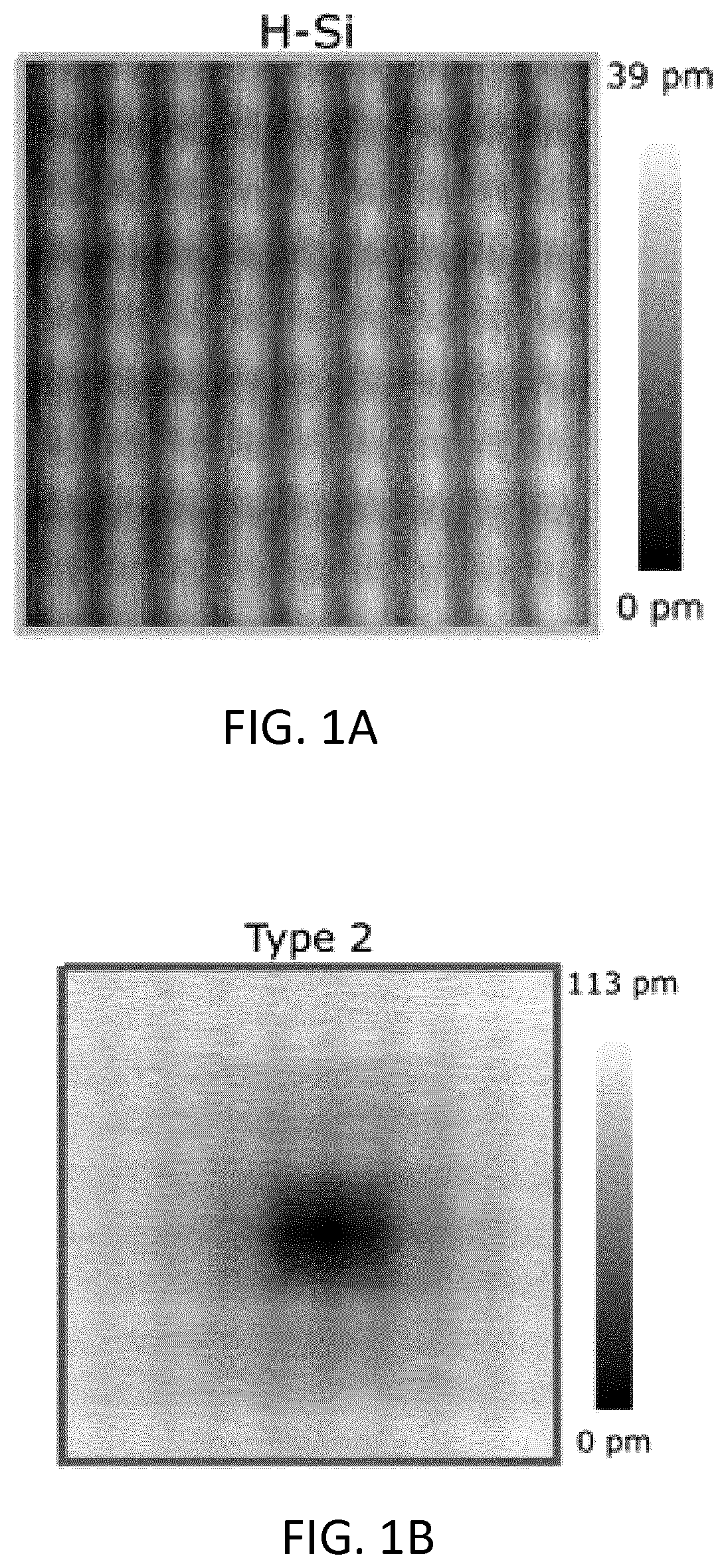
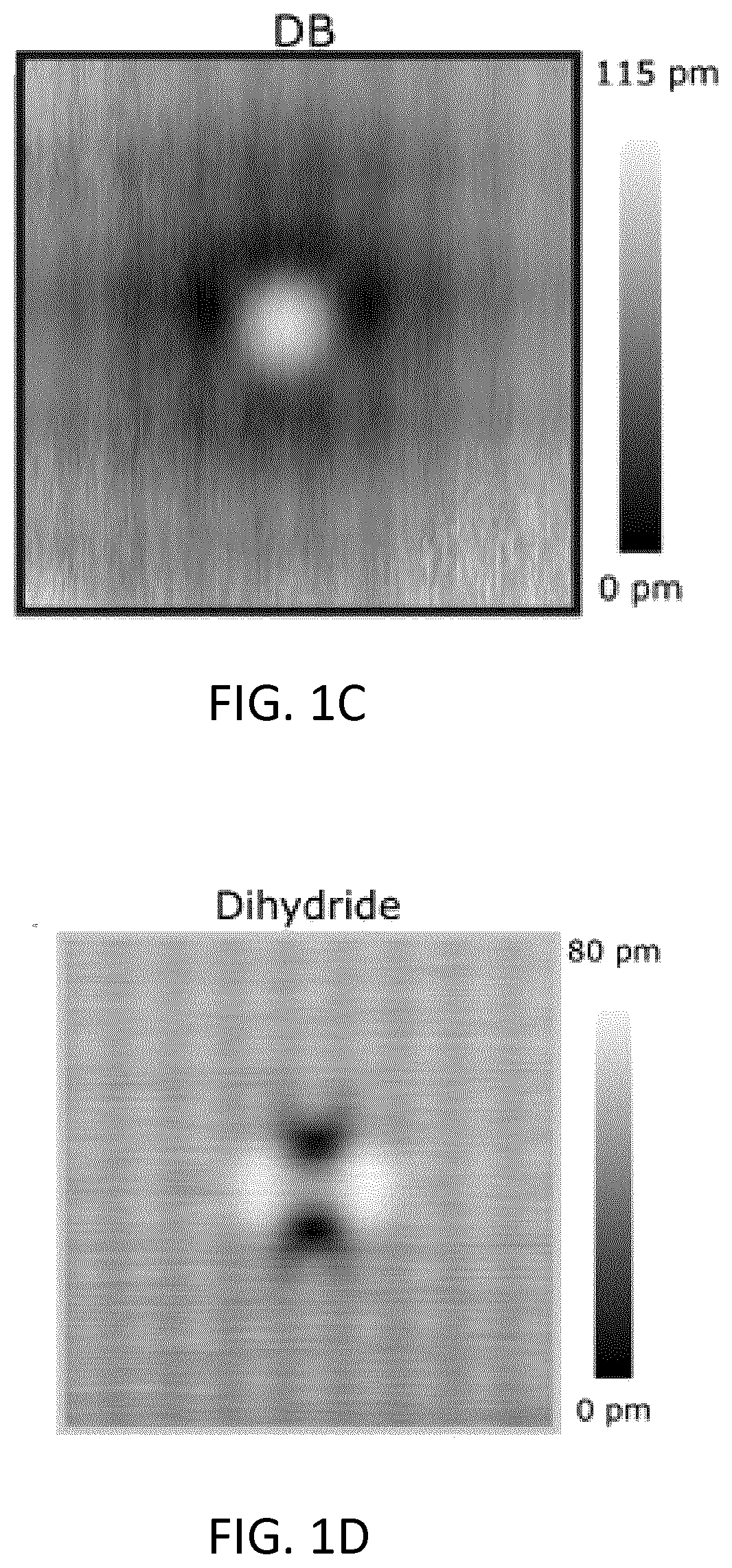
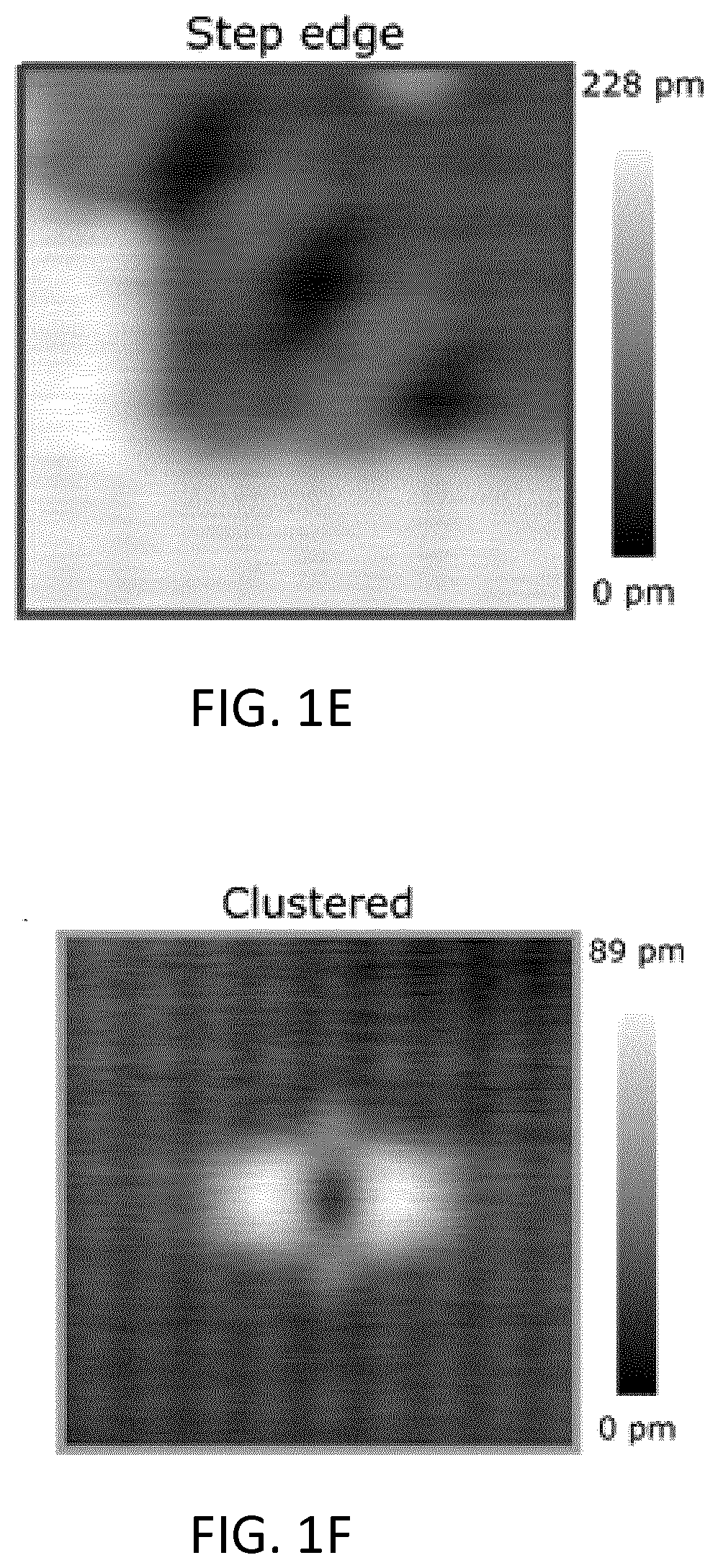
[0038]Samples used are highly arsenic doped (1.5×10⁻¹⁹ atoms / cm3) Si(100). Samples are degassed at 600° C. overnight followed by flash annealing at 1250° C. The samples are then terminated with hydrogen by exposing them to atomic hydrogen gas at 330° C.

[0039]Image and data acquisition are done using a Nanonis SPM controller and software. All training data is acquired at an imaging bias of either 1.3 V or 1.4 V with a tunneling current of 50 μA. The patterning automation r...


PUM


Abstract

A method for autonomously applying a dangling bond pattern to a substrate for atom scale device fabrication includes inputting the pattern, initiating a patterning process, scanning the substrate using a scanning probe microscope (SPM) to generate an SPM image of the substrate, feeding the SPM image into a trained convolution neural network (CNN), analyzing the SPM image using the CNN to identify substrate defects, determining a defect free substrate area for pattern application; and applying the pattern to the substrate in that area. An atom scale electronic component includes functional patches on a substrate and wires electrically connecting the functional patches. Training a CNN includes recording a Scanning Tunneling Microscope (STM) image of the substrate, extracting images of defects from the STM image, labeling pixel-wise the defect images, and feeding the extracted and labeled images of defects into a CNN to train the CNN for semantic segmentation.

Description

RELATED APPLICATIONS[0001]This application claims priority benefit of U.S. Provisional Application Ser. No. 62 / 806,381 filed on Feb. 15, 2019, the contents of which are hereby incorporated by reference.FIELD OF THE INVENTION[0002]The present invention is directed in general to atomic structures, and in particular to manufacturing of atomic structures based on machine learning technology to locate surface features on a substrate and pattern predefined atomic structures in defect-free areas of the surface to provide automated atomic scale fabrication.BACKGROUND[0003]With the miniaturization of complementary metal-oxide-semiconductor (CMOS) technology approaching its fundamental limit, alternatives built at an atomic level have been developed such as those disclosed in U.S. patent application Ser. No. 16 / 318,262.1,2,3 [0004]Scanning probe microscopes (SPMs) are a family of tools used to make images of nanoscale surfaces and structures, including atoms. They use a physical probe to scan...

Claims


Application Information

Patent Timeline
IPC IPC(8): G06T7/00G01Q30/04
CPCG06T7/0008G01Q30/04G06T2207/20081G01Q60/10G06T2207/30148G06T2207/10061G06T2207/20084G06N3/08B82B3/0019G06N3/048G06N3/045B82B3/00G06N3/02H01L29/02B82Y40/00
Inventor RASHIDI, MOHAMMADCROSHAW, JEREMIAHWOLKOW, ROBERT
Owner QUANTUM SILICON INC
Why Eureka
Try Eureka