Silicon carbide mosfet transistor device with improved characteristics and corresponding manufacturing process
- Summary
- Abstract
- Description
- Claims
- Application Information
AI Technical Summary
Benefits of technology
Problems solved by technology
Method used
Image

Examples
Embodiment Construction
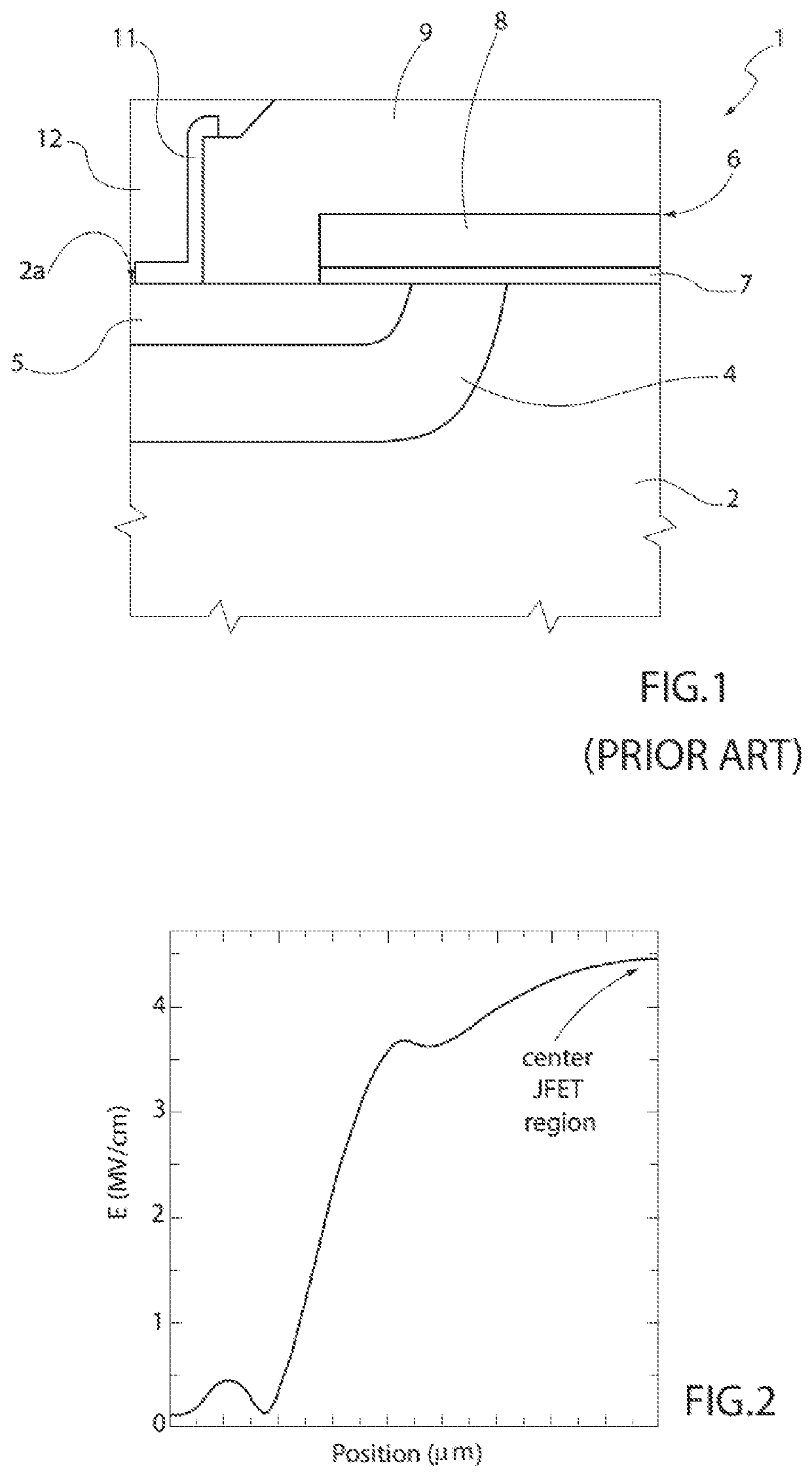
[0033]As will be described in detail in what follows, an aspect of the present solution envisages a reduction of the electrical field in the gate dielectric region, in particular in reverse-biasing conditions, by introducing a modified-doping region in the JFET region of the MOSFET device (the latter being in particular a 4H-SiC polytype silicon carbide power MOSFET transistor). The modified-doping region is a region having a net concentration of dopant reduced as compared to the concentration of the epitaxial layer in which the JFET region is provided.
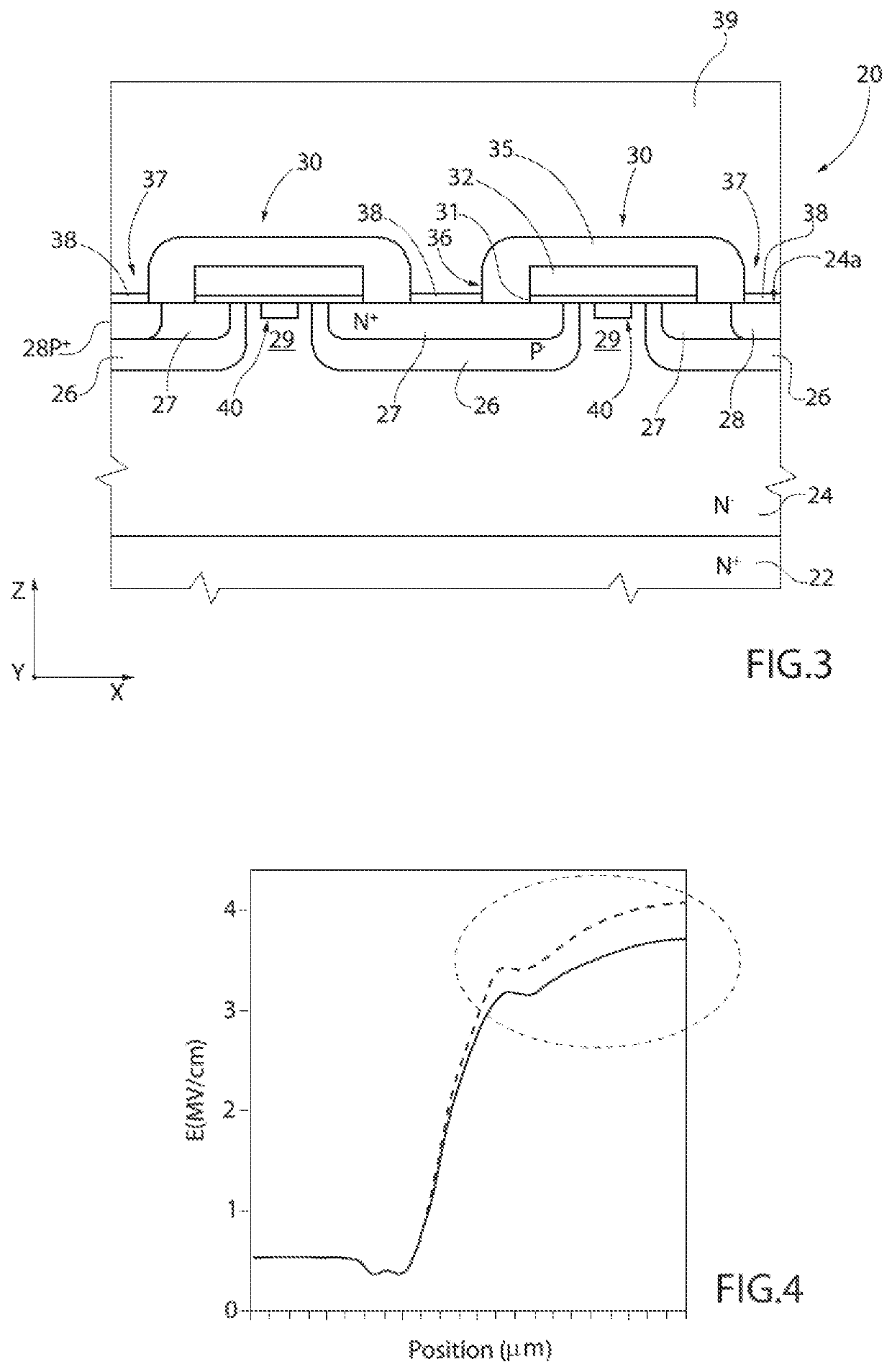
[0034]FIG. 3 shows a MOSFET device 20, in particular an N-channel vertical transistor for high-power application.
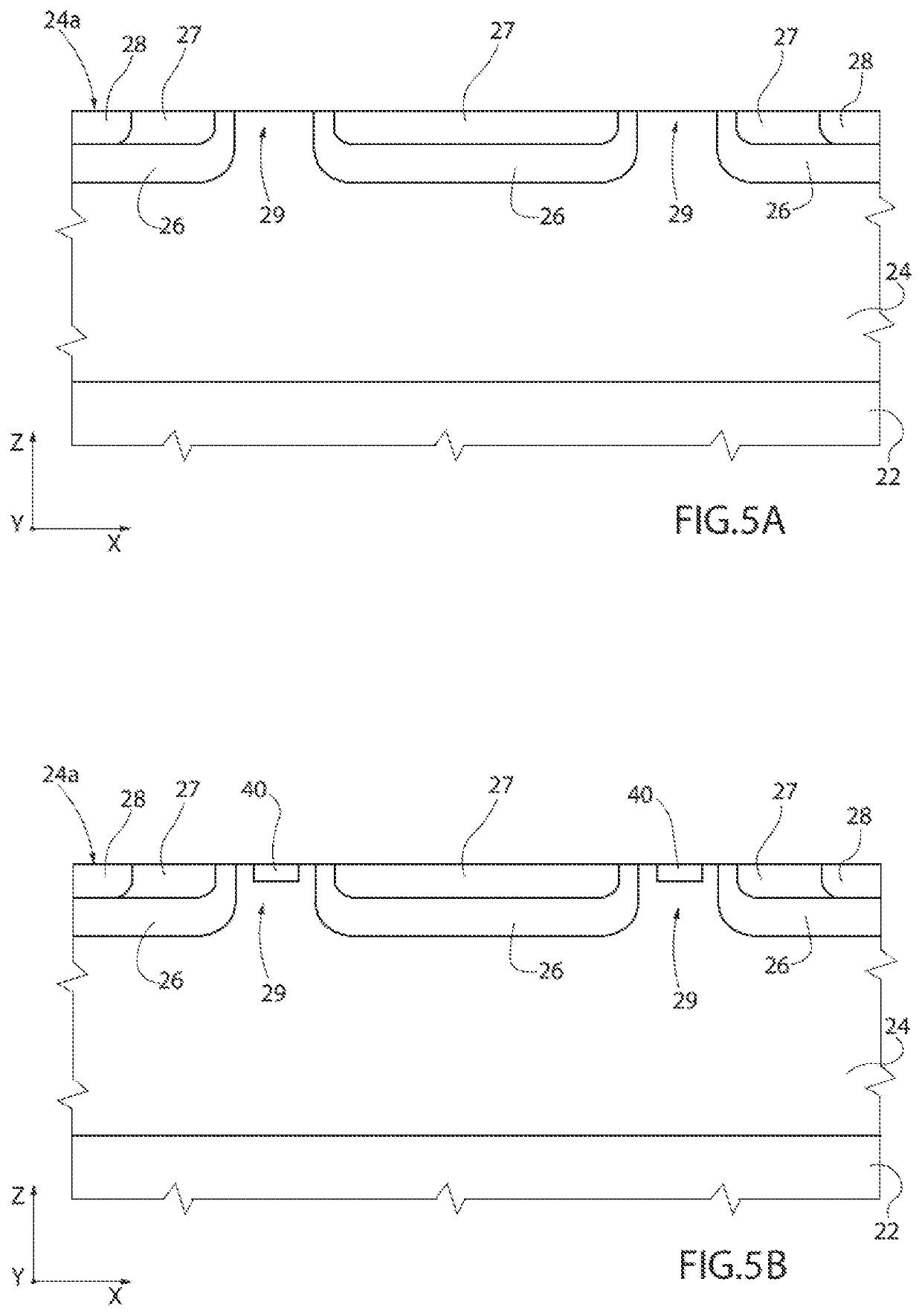
[0035]The MOSFET device 20 is provided in a die of semiconductor material, in particular of silicon carbide (more in particular of a 4H-SiC polytype), and comprises a substrate (or structural layer) 22, which is heavily doped (with doping of an N+ type), and a functional layer 24, arranged on the substrate 22 and having the...
PUM
 Abstract
Description
Claims
Application Information
 - R&D Engineer
- R&D Manager
- IP Professional
- Industry Leading Data Capabilities
- Powerful AI technology
- Patent DNA Extraction
Browse by: Latest US Patents, China's latest patents, Technical Efficacy Thesaurus, Application Domain, Technology Topic.
© 2024 PatSnap. All rights reserved.Legal|Privacy policy|Modern Slavery Act Transparency Statement|Sitemap