Low-voltage punch-through transient suppressor employing a dual-base structure

a transient suppressor and low-voltage technology, applied in the field of low-voltage punch-through transient suppressor employing a dual-base structure, can solve the problems of large leakage current, high cost, and high risk of electrical circuitry designed to operate at supply voltages less than 5 volts

Inactive Publication Date: 2000-01-18
SEMTECH CORP
View PDF4 Cites 46 Cited by
  • Summary
  • Abstract
  • Description
  • Claims
  • Application Information

AI Technical Summary

Problems solved by technology

Electronic circuitry which is designed to operate at supply voltages less than 5 volts are extremely susceptible to damage from overvoltage conditions caused by electrostatic discharge, inductively coupled spikes, or other transient conditions from its operating environment.
These devices perform well at voltages of 5 volts and above but run into problems when scaled to clamp below 5 volts.
The two major drawbacks incurred by using this device structure are very large leakage curre

Method used


Image

  • Low-voltage punch-through transient suppressor employing a dual-base structure
  • Low-voltage punch-through transient suppressor employing a dual-base structure
  • Low-voltage punch-through transient suppressor employing a dual-base structure

Examples


Embodiment Construction

Those of ordinary skill in the art will realize that the following description of the present invention is illustrative only and not in any way limiting. Other embodiments of the invention will readily suggest themselves to such skilled persons.

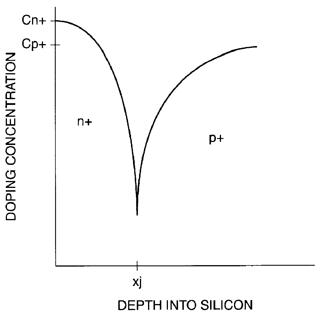
Reversed biased p+n+ zener diodes are currently the most widely-used devices for low voltage protection. These devices perform satisfactorily at voltages of 5 volts and above but exhibit very large leakage currents and high capacitance, two major drawbacks, when designed to clamp below 5 volts. FIG. 1. depicts the impurity doping profile of a typical low voltage pn junction device.

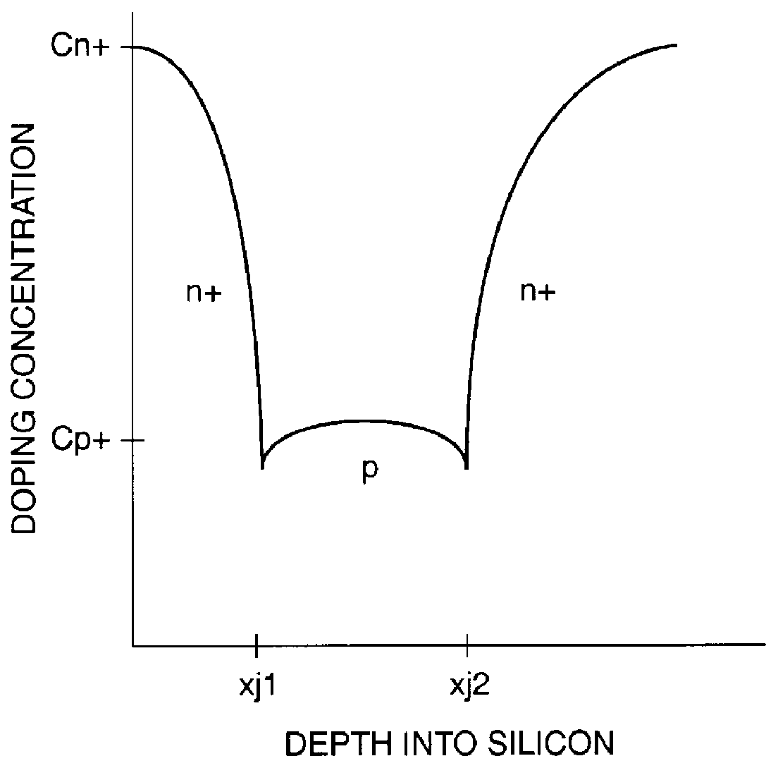
The n+pn+ uniform base punch-through diode is a second device capable of clamping low voltages. While the leakage and capacitance characteristics of the punch-through diode are superior to the conventional pn diode, the punch-through diode has poor clamping characteristics at high currents. The doping profile of a low voltage n+pn+ uniform base punch-through diode i...


PUM


Abstract

A punch-through diode transient suppression device has a base region of varying doping concentration to improve leakage and clamping characteristics. The punch-through diode includes a first region comprising an n+ region, a second region comprising a p- region abutting the first region, a third region comprising a p+ region abutting the second region, and a fourth region comprising an n+ region abutting the third region. The peak dopant concentration of the n+ layers should be about 1.5E18 cm-3, the peak dopant concentration of the p+ layer should be between about 1 to about 5 times the peak concentration of the n+ layer, and the dopant concentration of the p- layer should be between about 0.5E14 cm-3 and about 1.OE17 cm-3. The junction depth of the fourth (n+) region should be greater than about 0.3 mu m. The thickness of the third (p+) region should be between about 0.3 mu m and about 2.0 mu m, and the thickness of the second (p-) region should be between about 0.5 mu m and about 5.0 mu m.

Description

1. Field of the InventionThe present invention relates to semiconductor devices. More particularly, the present invention relates to a low-voltage punch-through transient suppressor employing a dual base structure.2. The Prior ArtElectronic circuitry which is designed to operate at supply voltages less than 5 volts are extremely susceptible to damage from overvoltage conditions caused by electrostatic discharge, inductively coupled spikes, or other transient conditions from its operating environment. The current trend of the reduction in circuit operating voltage dictates a corresponding reduction in the maximum voltage that the circuitry can withstand without incurring damage. As operating voltages drop below 5 volts to 3.3 volts and below it becomes necessary to clamp transient voltage excursions to below five volts.The most widely used device currently in use for low voltage protection is the reversed biased p+n+ zener diode. See O. M. Clark, "Transient voltage suppressor types a...

Claims


Application Information

Patent Timeline
IPC IPC(8): H01L29/66H01L29/866H01L29/861
CPCH01L29/8618H01L29/866H01L29/861
Inventor YU, BINHU, CHENMINGKING, YA-CHINPOHLMAN, JEFFREY T.TRIVEDI, RITA
Owner SEMTECH CORP
Why Eureka
Try Eureka