Electrostatic chuck

Inactive Publication Date: 2000-02-22
KYOCERA CORP
View PDF11 Cites 91 Cited by
  • Summary
  • Abstract
  • Description
  • Claims
  • Application Information

AI Technical Summary

Problems solved by technology

However, film forming and etching are carried out under the vacuum condition normally at 1.times.10.sup.-3 torr or lower, but when the semiconductor wafer 100 is electrostatically sucked to the holding surface 25 using the electrostatic chuck 21 as shown in FIG. 3 and He or other gas is supplied to the groove 26 of the holding surface 25, this gas flows out from the clearance between the semiconductor wafer 100 and the holding surface 25 to the inside of the chamber and the vacuum inside the chamber is lost, giving rise to a problem of detrimental effects on the accuracy of film-forming to the semiconductor wafer 100 or processing accuracy.
Even if any chipping or cracking is not generated at the edge of the convex portion 27', excessively rough profile irregularity of the top surface has a possibility to allow He or other gas to leak.
On the other hand, excessively large width of the outermost circumferential convex portion 27' in contact with the peripheral

Method used


Image

  • Electrostatic chuck
  • Electrostatic chuck
  • Electrostatic chuck

Examples


Example

(Embodiment 1)

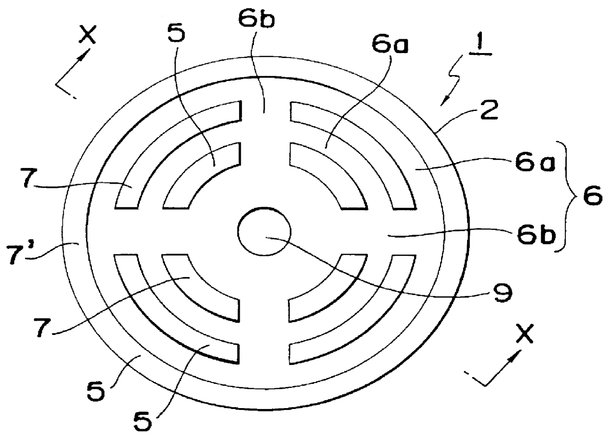
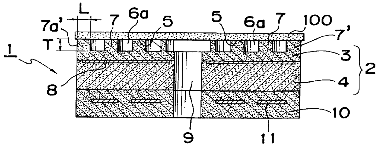
Now, an electrostatic chuck 1 made of aluminum nitride with a groove 6 shown in FIG. 1 was trially made and experiments were carried out to check for any sign of leakage when He gas was supplied to the groove 6 with a semiconductor wafer 100 sucked and held.

For the electrostatic chuck 1 used for the experiment, a slurry was prepared by adding a binder as a solvent to the pulverized high-purity aluminum nitride, then, a plurality of green sheets were formed by a tape forming method such as the doctor blade method, and to one of these green sheets, a tungsten paste with pulverized aluminum nitride added was printed by the screen printing process, then, the remaining green sheets were laminated in such a manner to cover the said tungsten paste and heat-pressurized at 50.degree. C. and at pressure of about 30 kg / cm.sup.2 to form a laminate, and the laminate was formed into a disk by machining. Then, the disk-form laminate was vacuum-degreased and then reduction-fired at ab...

Example

(Embodiment 2)

Then, electrostatic chucks 1 with the top surface of the convex portion 7' on the outermost circumference made to 0.1, 0.2, 0.3, and 0.4 .mu.m in terms of center line average roughneee (Ra) were prepared and measurements were carried out to check for any sign of leakage of He gas in the same manner as in the case of Embodiment 1.

Measurements were carried out with the width L of the convex portion 7' on the outer most circumference to be 1 mm and at the same time the chamber inside held to vacuum of 1.0.times.10.sup.-5 torr or lower.

The results indicate that no leakage of He gas was observed with the case in which the center line average roughness (Ra) of the top surface of the convex portion 7' was 0.3.mu.m or less, and the initial vacuum condition was able to be held, but with the center line average roughness (Ra) of the top surface of the convex portion 7' was 0.4 .mu.m, the vacuum inside the chamber lowered to 100 torr and leakage of He gas was observed.

This indica...

Example

(Embodiment 3)

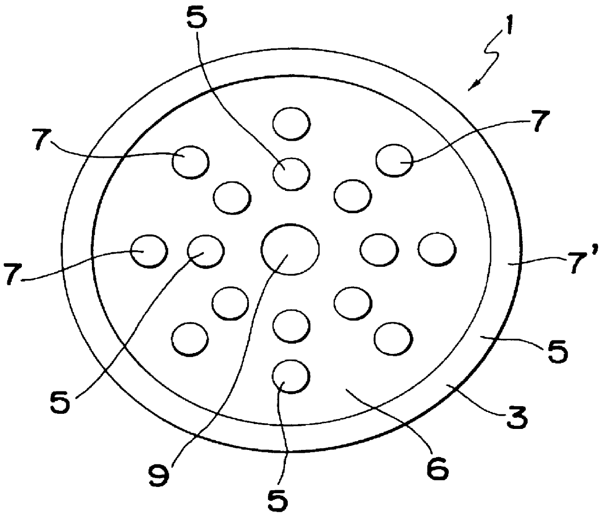
In addition, electrostatic chucks 1 with the groove 6 depth T of the dielectric layer 3 made to be 3, 5, 10 and 30 .mu.m were prepared, and the semiconductor wafer 100 was sucked and held, and then the rate of foreign matter adhering to the semiconductor wafer 100 was measured with a particle counter.

In this experiment, the electrostatic chucks in which the rate of foreign mater adhering to the semiconductor wafer was 250 or less were accepted because it is the number of particles required in manufacturing the semiconductor equipment.

Table 4 shows the results, respectively.

The results indicate that it was able to suppress the number of particles of foreign matter adhering to the wafer 100 to about 200 pcs, because sufficient distance was provided to the wafer 100 when the groove 6 depth T was 5 .mu.m or more. In contrast, with electrostatic chucks with the groove 6 depth T of 3 .mu.m, foreign matter on the groove 6 bottom surface was attracted by electrostatic suction ...


PUM


Abstract

In an electrostatic chunck with grooves formed on the dielectric layer surface, the rate of foreign matter adhering to the semiconductor wafer is reduced and at the same time the semiconduticor wafer can be uniformly heated without causing leakage of lie or other gases supplied to the grooves of the said holding surface into the chamer. The electrostatic chuck is composed of a dielectric layer made from ceramics or sapphire which has electrostatic electrodes, holding surface positioned on a same plane and concave spaces positioned next to the holding surface, at least one of the said holding surface being circumference, and the outermost such holding surface having a width of 1-20 mu m and being a smooth surface having a center line average roughness (Ra) of 0.3 mu m or less.

Description

1. Field of the InventionThe present invention relates to an electrostatic chuck used to hold semiconductor wafers in the semiconductor manufacturing process.2. Description of the Prior ArtHitherto, for the film-forming equipment for affixing film to semiconductor wafers or the etching equipment for carrying out details on semiconductor wafers in manufacturing process of the semiconductor facilities, an electrostatic chuck is used for a jig to hold semiconductor wafers at high accuracy.For this kind of electrostatic chuck there existed electrostatic chucks comprising an electrostatic electrode 28 embedded inside the ceramic base substrate 22 formed integral with a dielectric layer 23 consisting of ceramics such as alumina, silicon nitride, or aluminum nitride with high insulation capability and a ceramic substrate 24, wherein on the surface of the said dielectric layer 23, grooves 26 were engraved to achieve unevenness, and the top surface of the convex portion 27 was used for a hol...

Claims


Application Information

Patent Timeline
IPC IPC(8): H01L21/67H01L21/683H02N13/00
CPCH01L21/6831H02N13/00Y10T279/23
Inventor KAMITANI, SATORU
Owner KYOCERA CORP
Why Eureka
Try Eureka