Method for forming interconnection structure

a technology of interconnection structure and cu (copper) is applied in the direction of semiconductor devices, semiconductor/solid-state device details, electrical devices, etc., and can solve the problems of lsi performance degradation, complex process, and difficulty in filling a space between interconnects without forming voids

Inactive Publication Date: 2000-03-21
NEC ELECTRONICS CORP
View PDF6 Cites 12 Cited by
  • Summary
  • Abstract
  • Description
  • Claims
  • Application Information

AI Technical Summary

Benefits of technology

In accordance with the method for forming the interconnection structure of the present invention, the copper interconnect having a low electric resistance can be realized. The high integration and the miniaturization of a semiconductor device can be further promoted by applying this method for formation of the copper interconnect structure.

Problems solved by technology

In the conventional interconnection process, the process becomes complicated with the progress of the multi-level interconnection structure because of the increase of the number of steps of the photolithography and the etching.
Further, the filling of a space between interconnects without forming a void is difficult because the coverage of the interlevel dielectric film becomes severe with the miniaturization of the pitch of the interconnects.
In the generation in which the line width is between 0.18 and 0.20 micronmeter, the line pitch becomes narrow and the increase of the capacitance between the interconnects is not negligible so that the performance deterioration of LSI may be caused due to the signal / propagation delay.
However, the etching of copper is difficult to be controlled, and as a result, the processing of copper to make an interconnect in accordance with a process similar to that employed for making the conventional Al interconnect is hardly practicable.
Although, in the above description, a problem about an electric resistance increase has been pointed out by taking the copper interconnect formation by means of the Damasin process as an example, this problem arises not only in the Damasin process but also in a conventional process consisting of depositing a copper layer, forming a copper interconnect by means of patterning, embedding an dielectric film and opening a via-hole.

Method used


Image

  • Method for forming interconnection structure
  • Method for forming interconnection structure
  • Method for forming interconnection structure

Examples


Embodiment Construction

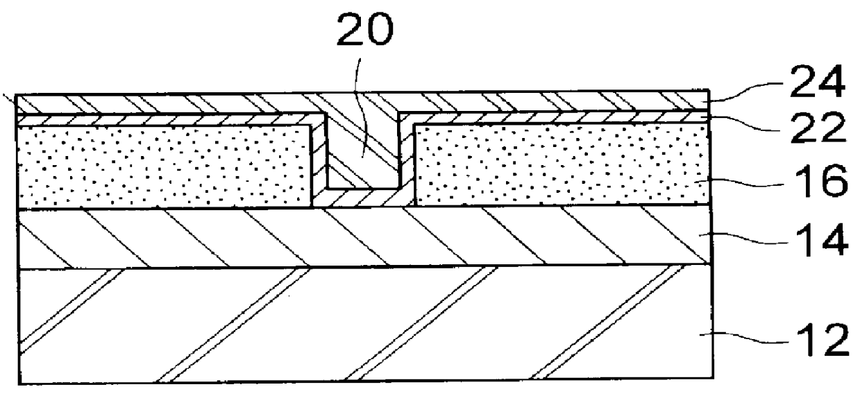
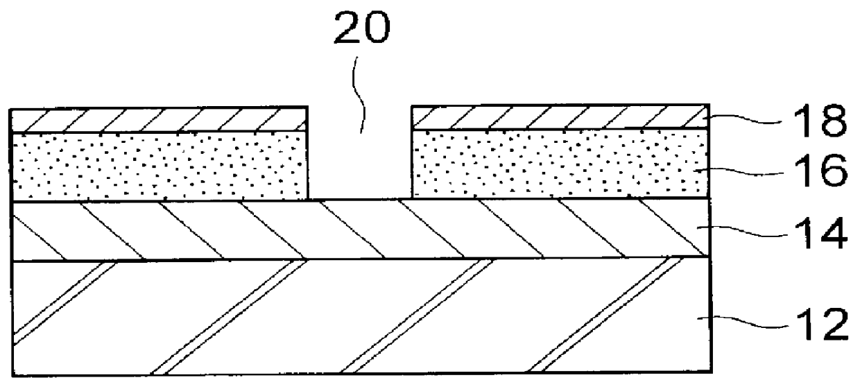
The present inventors have found the following by researching reasons of elevating an electric resistance of a copper interconnect when a copper multi-level interconnection structure is formed by the conventional Damasin process.

In the conventional copper interconnect formation process, as mentioned earlier, the surfaces of the via-hole and of the first level copper interconnect 24 are cleaned by washing the substrate when the tungsten plug is formed. Then, in order to exclude the moisture entering into the SiO.sub.2 film 16, the substrate is thermally treated in the thermal treatment furnace. After the substrate is taken out from the furnace, the substrate is conveyed to an apparatus for forming a tungsten blanket in order to embed the tungsten plug in the via-hole.

The present inventors have found during the researches that the electric resistance of the first level copper interconnect and of the electric connection with the tungsten plug elevate because the surface layer of the co...


PUM

PropertyMeasurementUnit
temperatureaaaaaaaaaa
thicknessaaaaaaaaaa
temperatureaaaaaaaaaa

Abstract

Disclosed herein is a method for forming a copper interconnect in which a substrate having the copper interconnect is exposed to atmosphere after the substrate is cooled to a temperature below 160 DEG C. under a non-oxidizable atmosphere. The exposure of the substrate to a relatively high temperature conventionally makes an electric resistance between interconnects on the substrate higher to prevent high integration. In accordance with the present invention, the above electric resistance can be reduced to smoothly realize the high integration because of the exposure of the substrate to a relatively low temperature.

Description

(a) Field of the InventionThe present invention relates to a method for forming a Cu (copper) interconnection structure for a semiconductor device on a substrate, and more in particular to a method for forming a minute multilevel interconnection structure of copper having a low electric resistance.(b) Description of the Related ArtA conventional and standard process of forming an interconnection structure in a semiconductor device includes forming a first level interconnect by processing a first level interconnect layer made of Al or an Al alloy by means of photolithography and etching, depositing an interlayer dielectric film on the first level interconnect, flattening the first level interconnect, forming a via hole, filling the via hole with tungsten, depositing a second level interconnect layer made of Al or an Al alloy and processing the second level interconnect layer by means of photolithography and etching.In the conventional interconnection process, the process becomes comp...

Claims


Application Information

Patent Timeline
Patent Type & Authority Patents(United States)
IPC IPC(8): H01L21/70H01L21/768H01L23/52H01L23/532H01L21/3205H01L23/522
CPCH01L21/76838H01L23/53238H01L2924/0002H01L2924/00H01L21/768
Inventor MATSUBARA, YOSHIHISA
Owner NEC ELECTRONICS CORP
Why Eureka
Try Eureka