Photovoltaic roofing element

a technology of photovoltaic roof and solar cells, applied in sustainable manufacturing/processing, greenhouse gas reduction, batteries, etc., can solve the problems of affecting the practical use of solar cells, cannot be freed from the danger of radioactivity, and the earth is warm, so as to achieve the effect of increasing the electrical resistan

Inactive Publication Date: 2000-05-16
CANON KK
View PDF35 Cites 44 Cited by
  • Summary
  • Abstract
  • Description
  • Claims
  • Application Information

AI Technical Summary

Benefits of technology

Still another object of the present invention is to provide a photovoltaic device wherein said transparent layer contains an impurity for increasing the electrical resistance.

Problems solved by technology

For most future energy sources, there are involved various problems, e.g. in the total reliance on fossil fuels such as petroleum and coal, the use of which is considered to result in warming of the earth because of the by-product carbon dioxide etc., and on nuclear power, which cannot be freed from the danger of radioactivity in case of an unpredictable accident or even in ordinary operation.
At present, however, there are some drawbacks that hinder practical use of such solar cells.
However, such solar cells, as an example of the known photovoltaic cells, require a large amount of energy and time for crystal growth and also require complex subsequent steps, so that mass production is difficult to achieve and supply thereof at a low price has therefore been difficult.
However, such thin film semiconductor photovoltaic devices have not been employed in practice because their conversion efficiency of light is lower than that of the crystalline silicon photovoltaic devices, and also their reliability under prolonged use has been low.
However, according to the experiences of the present inventors, such improvements have not been attained in most cases.
Also, under certain conditions of semiconductor deposition, the obtained solar cell does not have enough reliability for use under the conditions of high temperature and high humidity, despite the presence of the transparent layer.
For these reasons, the thin film solar cells have not been employed in practical applications, though they have the possibility of low cost production.

Method used


Image

  • Photovoltaic roofing element
  • Photovoltaic roofing element
  • Photovoltaic roofing element

Examples


experiment 1

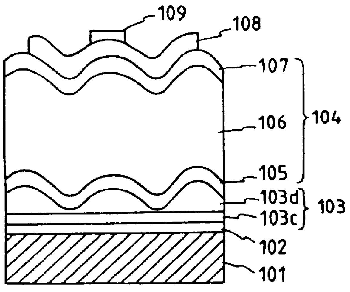
On a 5.times.5cm stainless steel plate (SUS 430), A1 was deposited to a thickness of 1500 .ANG. by DC magnetron sputtering, with the substrate at room temperature. Then ZnO was deposited to a thickness of 4000 .ANG. by DC magnetron sputtering, with a substrate temperature of 250.degree. C. Under SEM observation, the Al surface was smooth and lustrous, while the ZnO surface was turbid, showing concentrated crater-shaped recesses with diameters in a range of 4000 to 6000 .ANG.. In this state the light reflectance was measured within a wavelength range of 6000 to 9000 .ANG.. On the thus-formed rear reflective layer, there was formed a semiconductor junction layer, by means of glow discharge decomposition, an n-type a-Si layer of a thickness of 200 .ANG. utilizing SiH.sub.4 and PH.sub.3 as the raw material gases, an i-type a-Si layer of a thickness of 4000 .ANG. utilizing SiH.sub.4 as the raw material gas, and a p-type microcrystalline (.mu.c) Si layer of a thickness of 100 .ANG. utiliz...

experiment 2

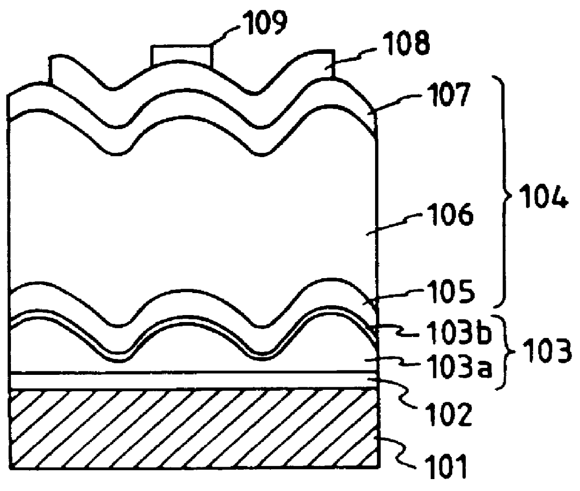
Sample 2a was obtained in the same wanner as Sample 1a in Experiment 1, except that Al was replaced by Ag and the current-collecting electrode was not formed.

Also, Sample 2b was prepared in the same manner as Sample 2a, except that the Ag deposition was conducted with a substrate temperature of 350.degree. C. instead of room temperature.

In Sample 2a, the entire rear reflective layer lacked lustre because the ZnO layer had an irregular surface structure although the Ag surface was smooth. In Sample 2b, the Ag surface had an irregular structure.

Table 2 shows the results of measurement of the conversion efficiency of both samples in a solar simulator of AM-1.5 light. Sample 2b showed a very low conversion efficiency, which is attributed to a short-circuiting, in consideration of the current-voltage characteristics. Also, in the SEM observation of both samples, Sample 2b showed scattered spot-shaped defects, and Auger analysis of these defect locations indicated Ag diffusion to the surf...

experiment 3

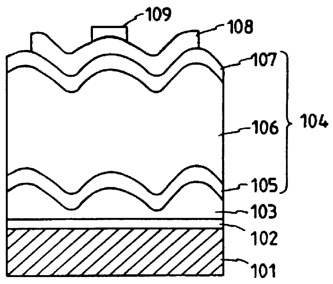
Sample 3a was prepared in the same manner as Sample 1a in Experiment 1, except that a-Si deposition was conducted in a deposition chamber which had been used for film deposition for a prolonged period without chamber cleaning.

Also, Sample 3b was prepared in the same manner as Sample 3a, except that the ZnO deposition was conducted with a ZnO target containing 0.5% of Cu.

Table 3 shows the results of measurement of the conversion efficiency of both samples in a solar simulator of AM-1.5 light. Both samples showed lower conversion efficiencies than in Sample 1a, under the influence of short-circuiting, particularly conspicuous in Sample 3a. In the SEM observation, both samples showed many pinholes in the a-Si layer. For reference, the resistivity of ZnO, measured by forming a chromium (Cr) electrode directly on the surface of the rear reflective layer and providing a weak current, was 5.times.10.sup.2 .OMEGA.cm in Sample 3a and 2.times.10.sup.5 .OMEGA.cm in Sample 3b. It is therefore c...


PUM

PropertyMeasurementUnit
temperatureaaaaaaaaaa
flatnessaaaaaaaaaa
heightaaaaaaaaaa

Abstract

A photovoltaic device comprises a metal with a smooth surface; a transparent conductive layer formed on the smooth surface; and a photoelectric conversion layer formed on the transparent conductive layer. The transparent conductive layer has an irregular surface at a side opposite to the smooth surface.

Description

BACKGROUND OF THE INVENTION1. Field of the InventionThe present invention relates to a photovoltaic device of a high conversion efficiency, high reliability and satisfactory mass producibility, and a method for producing the same, and it also relates to a secondary battery, an artificial satellite, a roofing material, a solar cell module, an automobile or the like, utilizing a solar cell as an example of said photovoltaic device.2. Related Background ArtFor most future energy sources, there are involved various problems, e.g. in the total reliance on fossil fuels such as petroleum and coal, the use of which is considered to result in warming of the earth because of the by-product carbon dioxide etc., and on nuclear power, which cannot be freed from the danger of radioactivity in case of an unpredictable accident or even in ordinary operation. In contrast, solar cells utilizing solar light as an energy source have very little influence on the environment, and are expected to be used ...

Claims


Application Information

Patent Timeline
Patent Type & Authority Patents(United States)
IPC IPC(8): H01L31/0392H01L31/058H01L31/075H01L31/048H01L31/06H01L31/036H01L31/052H01M10/42H01L31/20H01M10/46H01L31/18B64G1/44E04D13/18B60R16/04H01L31/04H01L31/076
CPCH01L31/03921H01L31/056H01L31/076H01L31/1884H01L31/206H01M10/465H02S40/38H02S20/23H01L31/048Y02B10/12Y02B10/70Y02E10/548Y10S136/291Y10S136/292Y10S136/293Y02E10/52Y02E10/541Y02E10/547Y02B10/10Y02P70/50Y02E60/10Y02E70/30H01L31/04H01L31/0236
Inventor TOYAMA, NOBORUNAKAGAWA, KATSUMI
Owner CANON KK
Why Eureka
Try Eureka