High density memory module with in-line bus switches being enabled in response to read/write selection state of connected RAM banks to improve data bus performance

a high-density memory module and data bus technology, applied in the direction of memory adressing/allocation/relocation, instruments, electrical apparatus construction details, etc., can solve the problems of limited number of memory "banks, high-density memory chips (e.g., 64 megabit (mb), 256 mb and greater) are either very expensive and/or not readily availabl

Inactive Publication Date: 2000-05-30
IBM CORP
View PDF25 Cites 172 Cited by
  • Summary
  • Abstract
  • Description
  • Claims
  • Application Information

AI Technical Summary

Problems solved by technology

However, the maximum system density often is artificially limited by one or more of the following:
The system has a limited number of memory "banks" (due to a lack of select lines from the memory controller).
High density memory chips (e.g., 64 megabit (Mb), 256 Mb and greater) are either very expensive and / or not readily available.
Previous solutions have been provided for all but the last of the above problems, but these solutions have been limited in applicability due to data line loading concerns.

Method used


Image

  • High density memory module with in-line bus switches being enabled in response to read/write selection state of connected RAM banks to improve data bus performance
  • High density memory module with in-line bus switches being enabled in response to read/write selection state of connected RAM banks to improve data bus performance
  • High density memory module with in-line bus switches being enabled in response to read/write selection state of connected RAM banks to improve data bus performance

Examples


Embodiment Construction

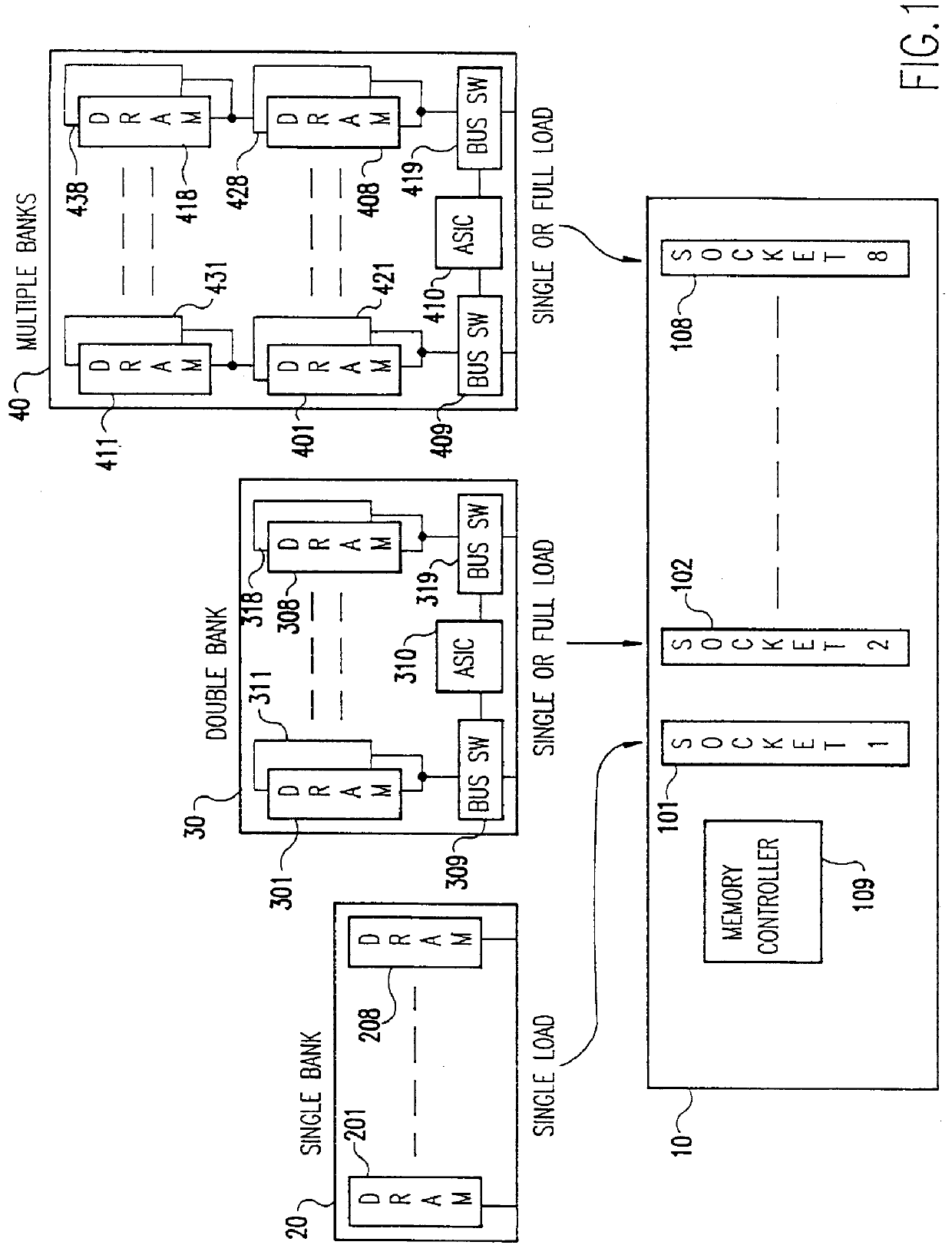
The invention will be described in terms of a specific implementation using dual in-line memory modules (DIMMs); however, those skilled in the art will recognize that other memory modules, such as single in-line memory modules (SIMMs), can be used in the practice of the invention. Such modules are typically implemented as a printed circuit card with tabs for insertion in a connector on a computer system board.

Referring now to the drawings, and more particularly to FIG. 1, there is shown a typical system board 10 with eight memory module sockets 101 to 108 and a memory controller 109. A conventional single bank DIMM 20 having, for example, eight 4 megabit (Mb) dynamic random access memory (DRAM) chips 201 to 208 may be plugged into any one of the sockets 101 to 108, usually beginning with socket 101 closest to the memory controller 109 and continuing in order until all the sockets 101 to 108 have a DIMM 20 inserted. Thus, for this example, the system board has a minimum configuration...


PUM


Abstract

Data line loading on high density modules with multiple DRAMs is minimized permitting the maximum memory density of systems of otherwise limited density to be increased without an ensuing performance degradation due to data line capacitive loading. First the single or dual in-line memory module (SIMM or DIMM) includes in-line bus switches. The bus switches are between the SIMM or DIMM module tabs (system) and random access memory devices (RAM) and are either in a high impedance (off) or active state depending on the READ/WRITE state of the RAM. When in the high impedance state, the effective loading of the module is that of the bit switch device. The logic for determining the READ/WRITE state may be embedded in an application specific integrated circuit (ASIC) that monitors bus activity and controls activation of the bus switches, be provided by a memory controller or, generated by the RAM itself. The bus switches are active when the RAM is performing a read or a write and inactive otherwise. The RAM is Fast Page Mode (FPM) and Extended Data Output (EDO) or Synchronous DRAM (SDRAM).

Description

1. Field of the InventionThe present invention generally relates to high density memory modules for computers and, more particularly, to multiple bank memory modules having minimal memory bus loading.2. Background DescriptionHigh density memory modules, e.g., single in-line memory modules (SIMMS) and dual in-line memory modules (DIMMs), continue to be in demand for high end personal computers (PCS), network servers and workstations, as added system performance can be achieved in many applications. However, the maximum system density often is artificially limited by one or more of the following:The system has a limited number of memory module "slots".The system has a limited number of memory "banks" (due to a lack of select lines from the memory controller).High density memory chips (e.g., 64 megabit (Mb), 256 Mb and greater) are either very expensive and / or not readily available.High density memory chips may have an operating voltage which is lower than the system memory interface v...

Claims


Application Information

Patent Timeline
Patent Type & Authority Patents(United States)
IPC IPC(8): G06F13/40G06F13/16G11C11/401H01L27/10G11C5/00
CPCG06F13/4068G06F12/06G06F13/38G06F13/10
Inventor CONNOLLY, BRIAN J.HAZELZET, BRUCE G.KELLOGG, MARK W.
Owner IBM CORP
Why Eureka
Try Eureka