Convex-microgranular surface structure

Inactive Publication Date: 2000-06-13
WASHI KOSAN
View PDF13 Cites 66 Cited by
  • Summary
  • Abstract
  • Description
  • Claims
  • Application Information

AI Technical Summary

Problems solved by technology

While this construction of antireflective layers is carried out using a vacuum vapor deposition equipment, a very large equipment is required for mass processing of lenses and this entails not only a high initial investment but also a high running cost both of which lead to appreciation of the lens cost.
However, it is quite difficult to form such microfine irregularities.
Since n.sub.1 and n.sub.2 are values determined according to the percentage volume of SiO.sub.2 within the immaginary plate, they might appear to be unrelated to the diameter of ultrafine particles but as experimentally demonstrated, production problems are encountered if the particle diameter is smaller than about 30 nm.
Thus, if the particle diameter is too small, the irregularities are too much smoothened out to lose the ability to inhibit reflection of light.
No suitable binder is available, either, for lens and other optical materials such as CR-39 and urethane resin.
The above technology was more or less satisfactory in that an original microgranular surface can be exactly transferred but when the transfer process was repeated, such troubles as dislodging of ultrafine particles, difficulty in mold release, and non-uniformity of the transfer surface occurred, so that the need for improvement was felt.
However, if the quantity of the binder is increased to prevent dislodging of particles, the ultrafine particles tend to be embedded in the binder to detract from the function of achieving a continuous

Method used


Image

  • Convex-microgranular surface structure
  • Convex-microgranular surface structure
  • Convex-microgranular surface structure

Examples


Embodiment Construction

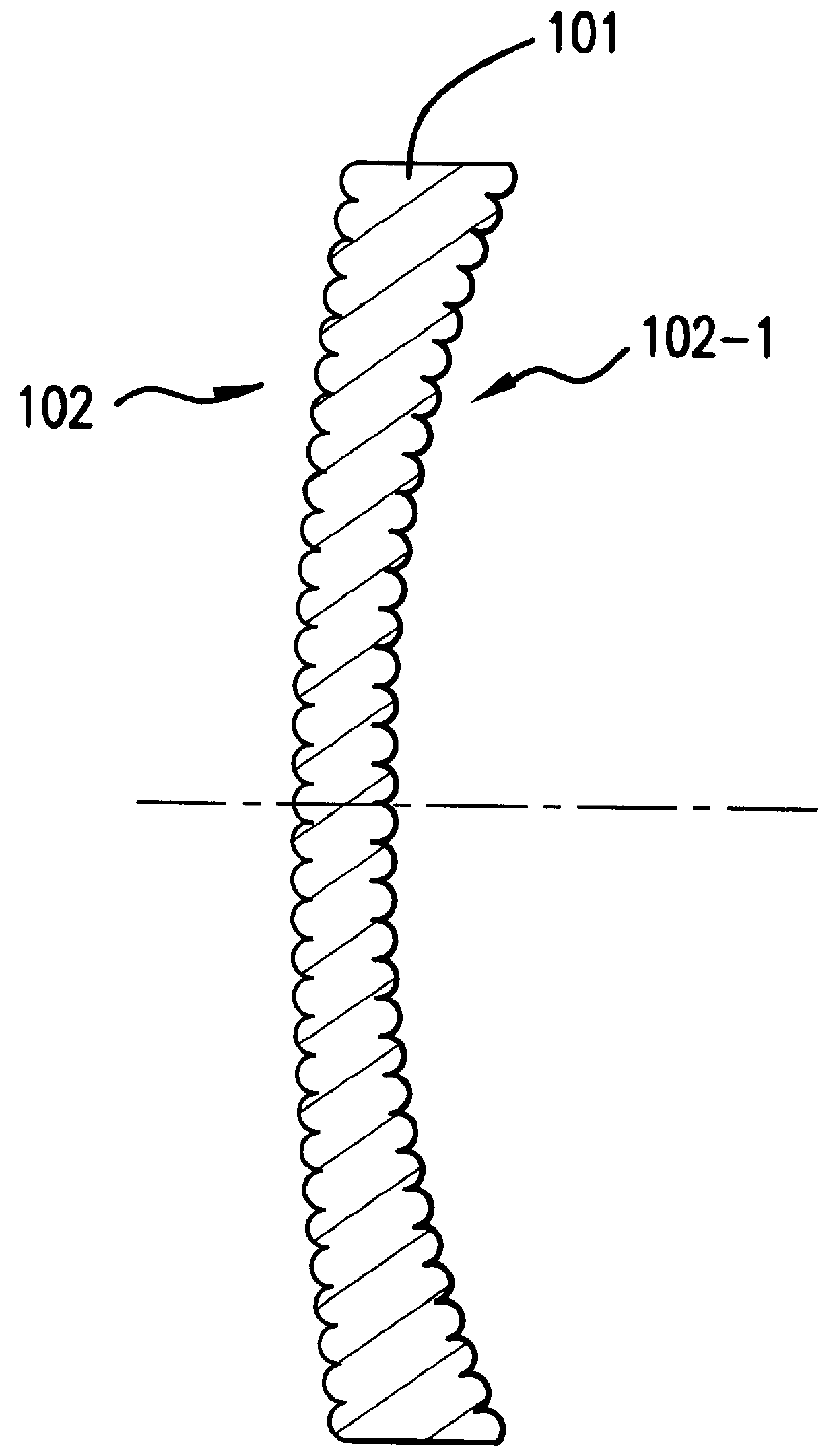
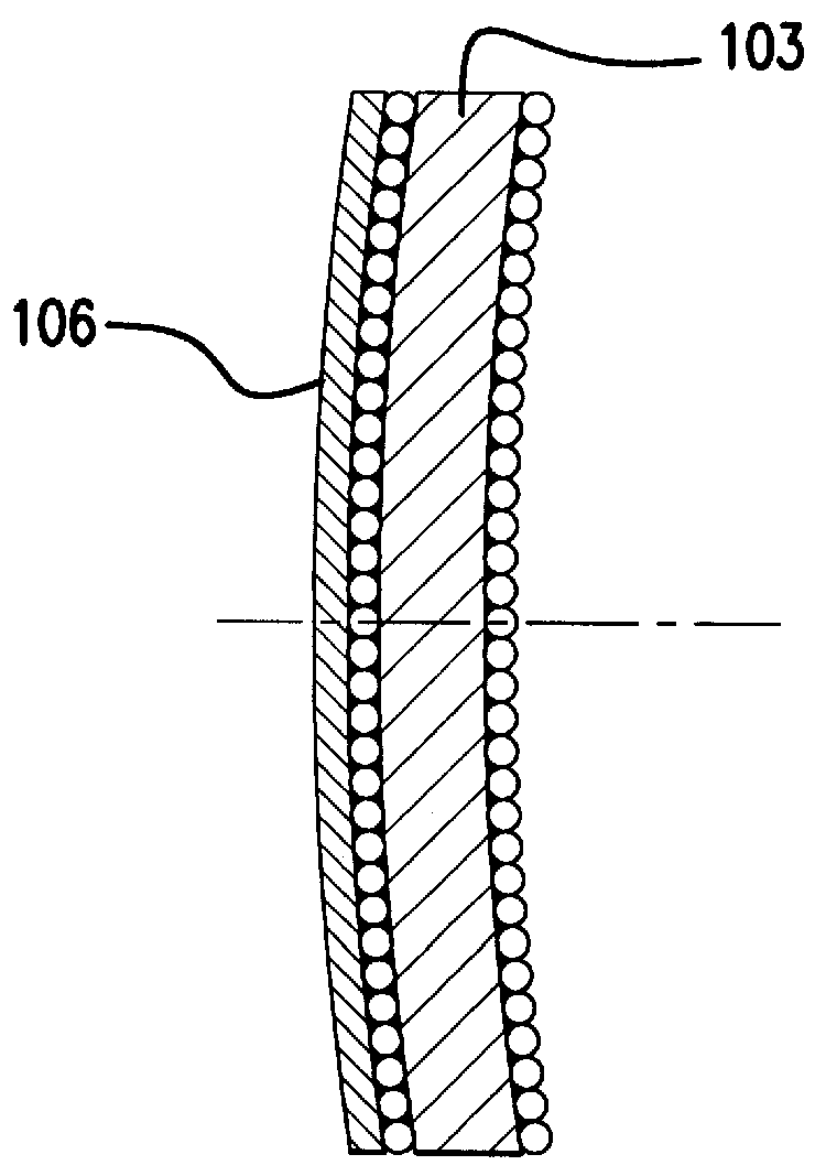
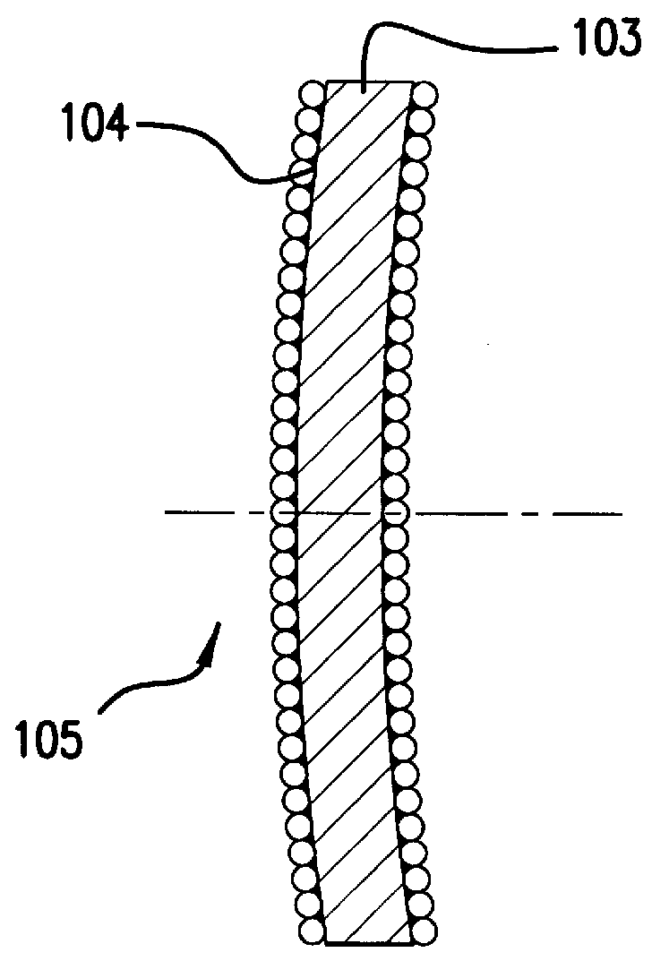
Referring to FIG. 1 which is a schematic cross-section view of a spectacle lens having microgranular surfaces formed by the transfer technique, the reference numeral 101 represents a lens body and the numeral 102 represents a transferred convex microgranular monolayer surface. FIG. 2 shows a cast polymerization glass mold 103 to which ultrafine SiO.sub.2 particles with a diameter of 120 nm have been firmly secured.

For the formation of the lens 101 shown in FIG. 1, the microgranular surface 105 on the convex side (FIG. 2) is cleaned thoroughly and a nickel VVD and a nickel plating are carried out in that order, followed by rotation of the mold in the plating bath so as to even out the thickness of the nickel plate. When the nickel plate 106 has been adjusted to a predetermined thickness, the mold is taken out from the plating bath, rinsed, and dried. Then, a mold 107 having the same radius of curvature as that of the nickel plate layer 106 is bonded (FIG. 4). The assembly is subjecte...


PUM

PropertyMeasurementUnit
Nanoscale particle sizeaaaaaaaaaa
Thicknessaaaaaaaaaa
Widthaaaaaaaaaa

Abstract

PCT No. PCT/JP96/00350 Sec. 371 Date Nov. 6, 1996 Sec. 102(e) Date Nov. 6, 1996 PCT Filed Feb. 16, 1996 PCT Pub. No. WO96/25677 PCT Pub. Date Aug. 22, 1996The surface and/or interface of a lens or the like is formed with a convex-microgranular surface. For this purpose, a stamper 108 having a concave-micro-granular transfer-molding surface transfer-molded from a convex-microgranular surface comprised of SiO2 or the like and varying continuously in the index of refraction is used to reproduce the convex-microgranular surface.

Description

The present invention relates to a convex-micro-granular surface structure which is contributory to attenuation of reflectance and / or enhancement of light collection. In further aspects, the present invention relates to a plastic lens structure for spectacle use, a process for manufacturing the same, a solar cell including a mechanism for improving the light collection efficiency, a technology for preventing surface reflection on the readout side of an optomagnetic recording medium, a photosensitive material which is chiefly used as a photographic film or printing paper, the light-receiving surface of which is provided with an antireflective function, a method and apparatus for preventing reflection of light within an irradiation light path in the fabrication of an electronic circuit including optical means, and associated products, among others.BACKGROUND TECHNOLOGYIn diverse industrial fields, attenuation of reflection and / or enhancement of light collection efficiency has been req...

Claims


Application Information

Patent Timeline
IPC IPC(8): G02B1/11G02B1/12G02B1/10G03C1/825G03F7/00G11B7/252G11B11/105G11B11/00G11B7/26G11B7/24H01L31/0232H01L31/052H01L31/0236H01L31/048B32B3/30G11B11/10H01L31/054
CPCG02B1/11H01L31/0547G02B1/12G03C1/825G03F7/0005G11B7/24G11B7/252G11B7/26G11B11/10582H01L31/0232H01L31/0236H01L31/048H01L31/0543G02B1/113G11B11/10584Y02E10/52H01L31/02366G02B1/10
Inventor ONO, KOTAROSUMIDA, KENJI
Owner WASHI KOSAN
Why Eureka
Try Eureka