Method of forming a self-aligned silicide MOSFET with an extended ultra-shallow S/D junction

a metal oxide semiconductor transistor and self-aligned technology, applied in the direction of semiconductor devices, electrical equipment, transistors, etc., can solve the problems of increased packing density of wafers, higher junction leakage, and salicide structure not being perfected

Inactive Publication Date: 2000-07-11
TAIWAN SEMICON MFG CO LTD +2
View PDF8 Cites 46 Cited by
  • Summary
  • Abstract
  • Description
  • Claims
  • Application Information

AI Technical Summary

Benefits of technology

FIG. 5 is a cross-sectional view of a semiconductor wafer illustrating the step of performing a high dosage S/D/G ion implantation and a second anneal step to form the stable silicide phase acco

Problems solved by technology

According to the trend of integrated circuits, the fabrication of the MOSFET also involves various issues such as short channel effect and the generation of parasitic capacitance.
With the advent of Ultra large Scale Integrated (ULSI) technologies, the sizes of semiconductor devices have gotten smaller and smaller than ever, resulting in the packing density of a wafer increasing continuously.
However, salicide structu

Method used


Image

  • Method of forming a self-aligned silicide MOSFET with an extended ultra-shallow S/D junction
  • Method of forming a self-aligned silicide MOSFET with an extended ultra-shallow S/D junction
  • Method of forming a self-aligned silicide MOSFET with an extended ultra-shallow S/D junction

Examples


Embodiment Construction

The present invention will be described in detail with reference to drawings. The purpose of the present invention is to provide a method for fabricating a self-aligned silicide metal oxide semiconductor transistor (MOSFET). The detailed processes will be described as follows.

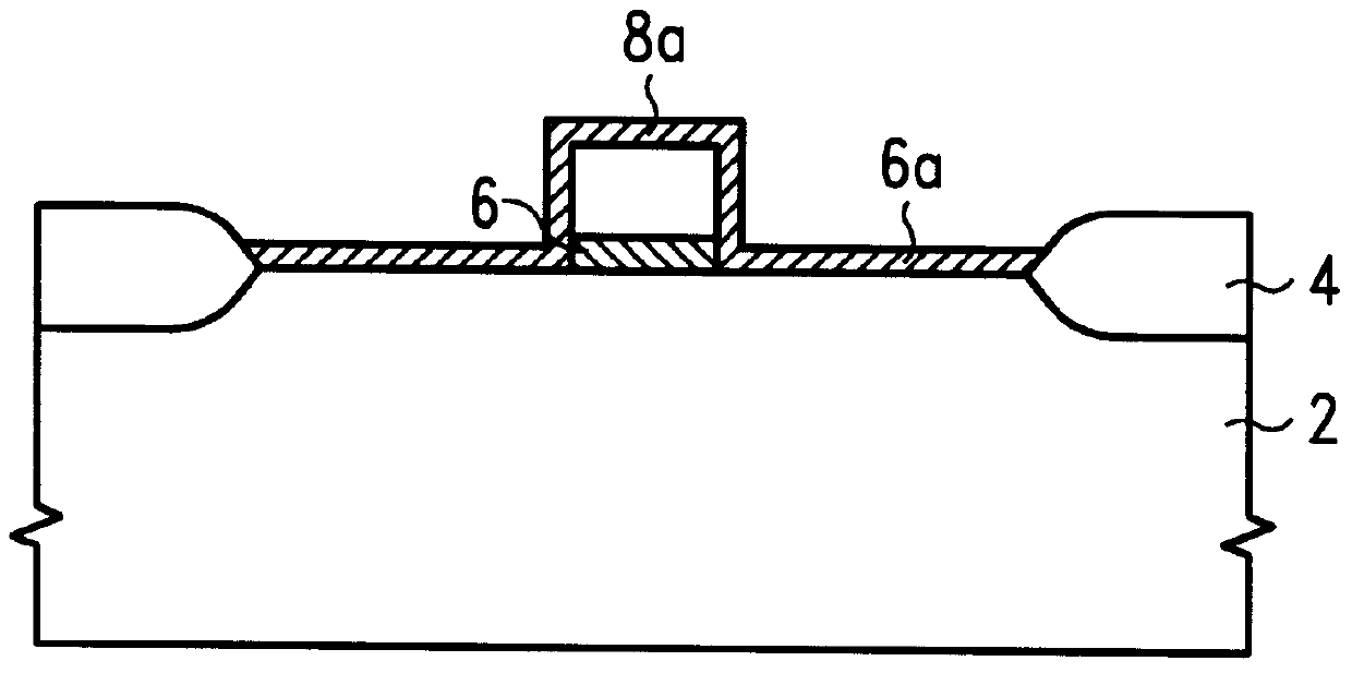
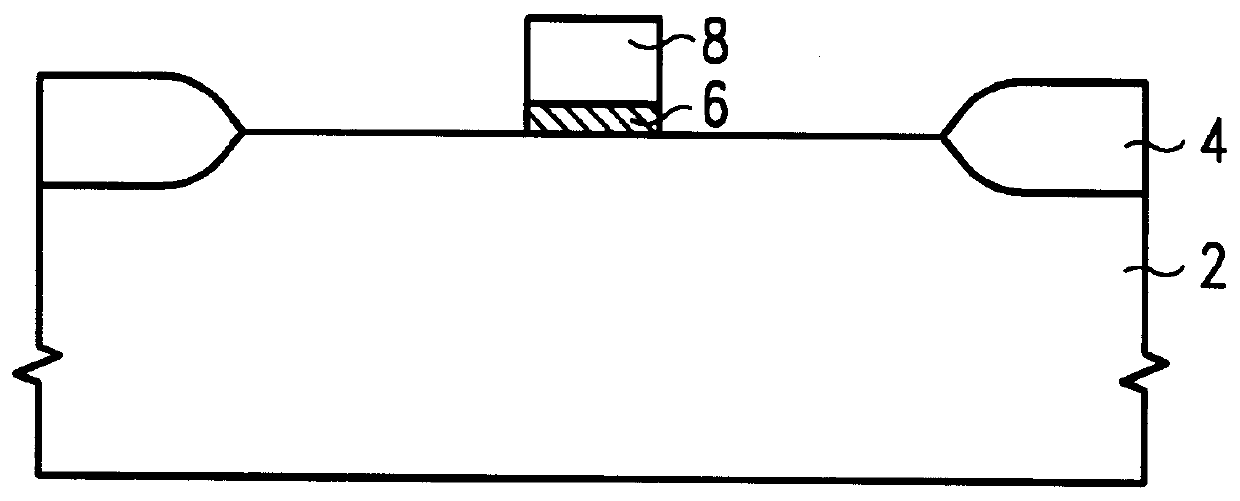
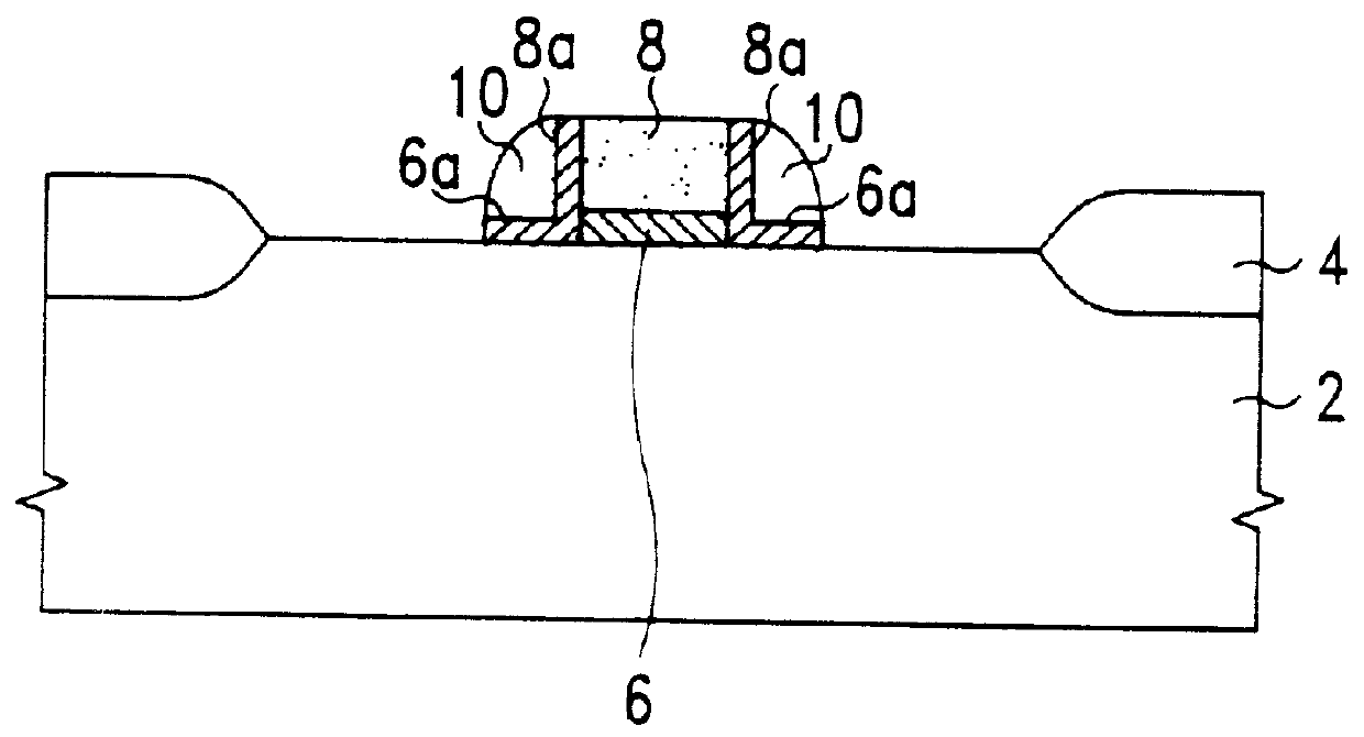
Referring to FIG. 1, in a preferred embodiment, a single crystal silicon substrate 2 with a crystallographic orientation is provided. A plurality of thick field oxide (FOX) regions 4 are formed to provided isolation between devices on the substrate. For example, the FOX regions 4 can be formed via lithography and etching steps to etch a silicon nitride-silicon dioxide composition layer. After the photoresist is removed and wet cleaned, thermal oxidation in an oxygen-steam environment is used to grow the FOX region 4 to a thickness of about 3000-8000 angstroms. The FOX region 4 can be replaced by a plurality of shallow trench isolations, as is well known in the art. Next, a silicon dioxide layer 6 is formed on ...


PUM


Abstract

The method of the present invention is a method of including forming a gate oxide layer on the substrate. A polysilicon layer is formed on the gate oxide layer. Then, a photographic and etching steps are used to form a gate structure. An oxidation is performed on the substrate and the gate structure to form an first oxide layer on the substrate and on the surface of the polysilicon gate. A silicon nitride layer is deposited on the first oxide layer. A side-wall spacers is formed on the side walls of the gate structure, a first portion of the first oxide layer remaining between the gate structure and the side-wall spacers, and a second portion of the first oxide layer remaining under the side-wall spacers. Next, a first ion implantation performed into the substrate to form first doped ions regions to serves as source and drain region of the transistor. Then, the side-wall spacers is removed, therefore remained the second portion of the first oxide layer covered by the side-wall spacers. Subsequently, a second ion implantation performed through the second portion of the first oxide layer to form second doped ion regions to serve as an extended source and drain region of the transistor. A rapid thermal annealing performed to form an extended source and drain junction and aligned to the region of the side-wall spacers being disposed.

Description

1. Field of the InventionThe present invention relates to a semiconductor device, especially to a method of fabricating a self-aligned silicide metal oxide semiconductor transistor (MOSFET) with an extended ultra-shallow S / D junction.2. Description of the Prior ArtMetal oxide semiconductor field effect transistors (MOSFETs) have been traditionally used and widely applied in the semiconductor technologies. According to the trend of integrated circuits, the fabrication of the MOSFET also involves various issues such as short channel effect and the generation of parasitic capacitance. One of the issues is hot carriers that will inject into gate oxide, which is has been overcome by the development of light doped drain (LDD) structure.The salicide with extension S / D junction structure has received a lot of attention, recently. With the advent of Ultra large Scale Integrated (ULSI) technologies, the sizes of semiconductor devices have gotten smaller and smaller than ever, resulting in the...

Claims


Application Information

Patent Timeline
IPC IPC(8): H01L21/265H01L21/02H01L21/336
CPCH01L21/2652H01L29/665H01L29/6659
Inventor WU, SHYE-LIN
Owner TAIWAN SEMICON MFG CO LTD
Why Eureka
Try Eureka