Semiconductor having large volume fraction of intermediate range order material

a technology of order materials and semiconductors, applied in the field of semiconductors, can solve the problems of limited semiconductor technology, difficult fabrication, limited properties,

Inactive Publication Date: 2000-07-11
BEKAERT ECD SOLAR SYST
View PDF10 Cites 35 Cited by
  • Summary
  • Abstract
  • Description
  • Claims
  • Application Information

AI Technical Summary

Problems solved by technology

In the earliest stages, semiconductor technology was limited by the use of single crystalline materials.
As a result single crystalline devices were expensive, difficult to fabricate and limited in their properties.
In some instances, one property of a given morphology and local order of semiconductor may be ideal for a particular purpose whereas the value of another property of that same material may not be so well suited.
For example, the aforenoted high optical absorption of amorphous silicon is ideal for a photovoltaic device; however, the fairly wide band gap of amorphous silicon does not permit it to address the longer wavelength portions of the solar spectrum.
The use of narrower band gap crystalline material in photovoltaic devices increases the portion of the useable light spectrum and the high conductivity, high mobility and long minority carrier diffusion length in crystalline silicon decreases the series resistance of the photovoltaic device, thereby increasing its overall efficiency; but, the trade-off is that crystalline cells are relatively thick because of their low absorption and hence they are fragile, bulky and expensive.

Method used


Image

  • Semiconductor having large volume fraction of intermediate range order material
  • Semiconductor having large volume fraction of intermediate range order material
  • Semiconductor having large volume fraction of intermediate range order material

Examples


Embodiment Construction

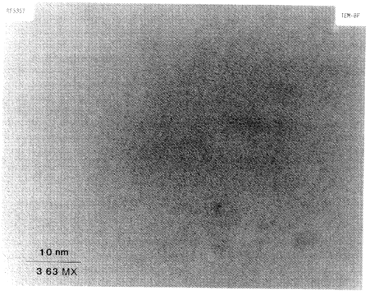
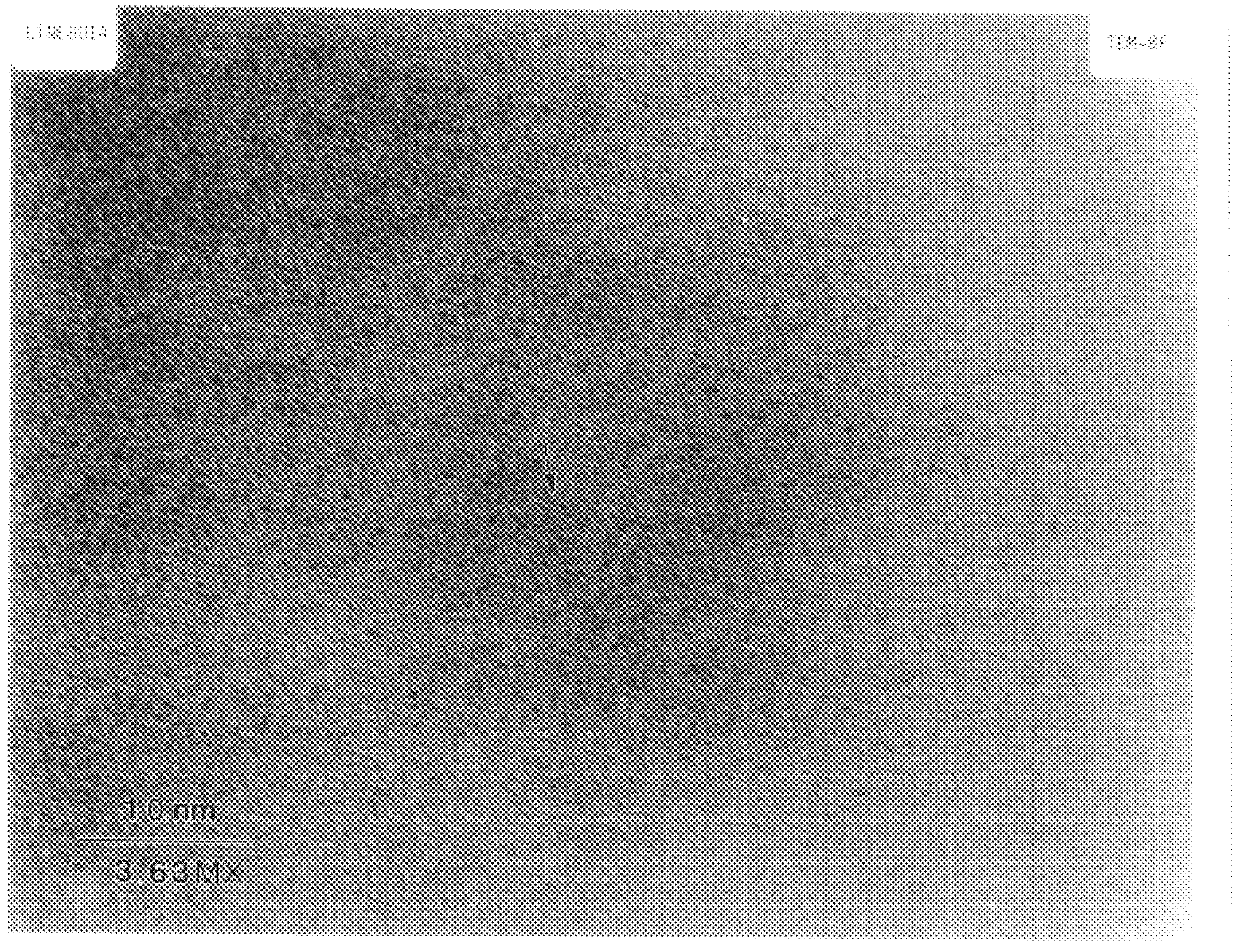
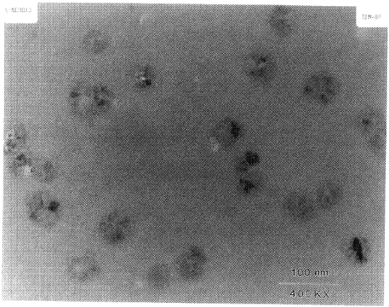
The existence of intermediate range order (IRO) material has been known since at least 1981. See for example a paper co-authored by one of the instant inventors, S. R. Ovshinsky, entitled "THE NATURE OF INTERMEDIATE RANGE ORDER IN SI:F:H:(P) ALLOY SYSTEMS", Tsu et al., Journal De Physique Colloque C4, No. 10, 42, pp. C4-269-72, October 1981. The instant inventors have been investigating the deposition of silicon materials by plasma enhanced chemical vapor deposition (PECVD) from disilane (Si.sub.2 H.sub.6) and hydrogen (H.sub.2). More recently they have investigated deposition using high hydrogen dilution. See for example "STABILITY STUDIES OF HYDROGENATED AMORPHOUS SILICON ALLOY SOLAR CELLS PREPARED WITH HYDROGEN DILUTION", Yang et al., Materials Research Society Symposium Proceedings, Vol. 336, pp. 687-92, 1994; and "HYDROGEN DILUTION EFFECTS ON a-Si:H AND a-SiGe:H MATERIALS PROPERTIES AND SOLAR CELL PERFORMANCE", Xu et al., International Conference on Amorphous Semiconductors (IC...


PUM

PropertyMeasurementUnit
crystallite sizesaaaaaaaaaa
band gapaaaaaaaaaa

Abstract

A high quality non-single-crystal silicon alloy material including regions of intermediate range order (IRO) silicon alloy material up to but not including the volume percentage required to form a percolation path within the material. The remainder of the material being either amorphous or a mixture of amorphous and microcrystalline materials. The materials were prepared by CVD using differing amounts of hydrogen dilution to produce materials containing differing amounts of IRO material. Preferably the material includes at least 8 volume percent of IRO material.

Description

FIELD OF THE INVENTIONThis invention relates to semiconductors in general. In particular, the invention relates to a semiconductor material having a volume fraction of intermediate range ordered materials (crystallite sizes 10-50 Angstroms) of up to, but not including, the volume percentage required to form a percolation path within the material.BACKGROUND OF THE INVENTIONWithin a relatively brief time, semiconductor materials have made possible the creation of a wide range of optical and electronic devices which have played a major role in the shaping of our world. The impact of semiconductor devices has been felt from the battlefield to the playground and from the kitchen to the cosmos. In the earliest stages, semiconductor technology was limited by the use of single crystalline materials. These materials were, of necessity, highly pure and possessed a morphology with extremely regular and long-range periodicity. The dual and interdependent constraints of periodicity and stoichiom...

Claims


Application Information

Patent Timeline
Patent Type & Authority Patents(United States)
IPC IPC(8): H01L31/20H01L31/18C23C16/24H01L21/205H01L21/336H01L29/786H01L29/861H01L31/02H01L31/028H01L31/04
CPCH01L31/204Y02E10/50Y02E10/547Y02P70/50H01L31/028
Inventor OVSHINSKY, STANFORD R.GUHA, SUBHENDUYANG, CHI-CHUNGDENG, XUNMINGJONES, SCOTT
Owner BEKAERT ECD SOLAR SYST
Why Eureka
Try Eureka