High emittance electron source having high illumination uniformity

a high-emittance, electron source technology, applied in the manufacture of discharge tubes/lamps, discharge tube main electrodes, electric discharge tubes/lamps, etc., can solve the problems of limited throughput of electron beams, additional problems, and limitations in resolution,

Inactive Publication Date: 2000-07-18
IBM CORP
View PDF15 Cites 17 Cited by
  • Summary
  • Abstract
  • Description
  • Claims
  • Application Information

AI Technical Summary

Problems solved by technology

Extreme ultra-violet (EUV) radiation and X-rays are being investigated but present additional problems.
However, some practical limitations on resolution are also characteristic of electron beams.
Therefore, throughput of an electron beam (hereinafter sometimes "e-beam") tool is limited by the beam current which can be developed.
Accordingly, high density of electron population in the electron beam causes aberrations in the nature of blurring or defocussing in the beam image because of the interactions between the electrons.
However, uniformity of electron emission is not of importance in any of these applications.
However, for larger cathodes, direct resistance heating is impractical because of the large currents which would be required.
However, heat losses to the mounting are significant and increased input power is required to compensate for that heat loss.
Moreover, configuration of the bombardment arrangement is not compatible with a uniform accelerating or extraction field, nor is a cathode material having uniform electron emission used.
Such alloying tends to weaken the filament.
Accordingly, it is seen that the current level of skill in the art does not answer a need for a high current cathode having a large area to support high emittance while maintaining uniformity of temperature and electron emission over the large cathode area.

Method used


Image

  • High emittance electron source having high illumination uniformity
  • High emittance electron source having high illumination uniformity
  • High emittance electron source having high illumination uniformity

Examples


Embodiment Construction

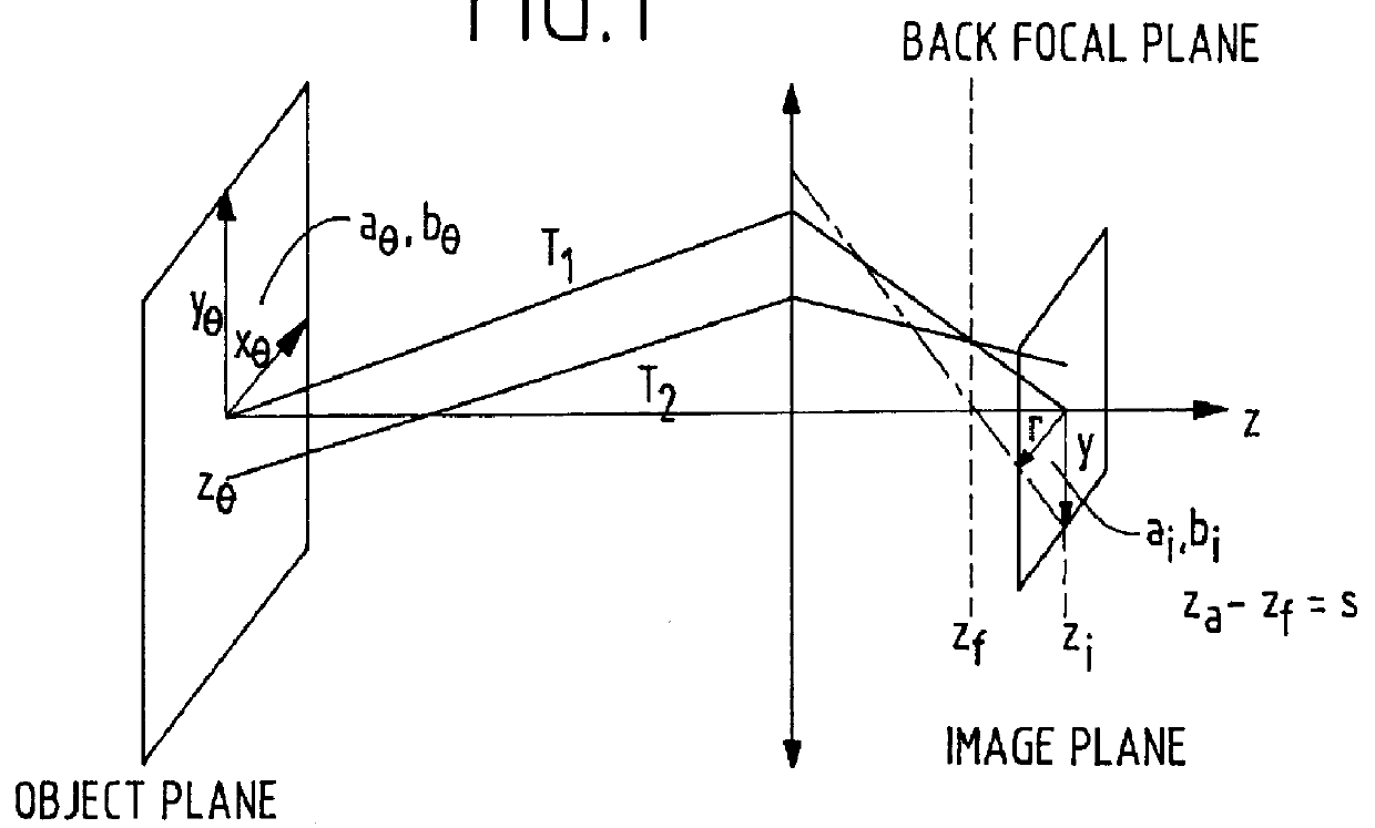
Referring now to the drawings, and more particularly to FIG. 1, a light-optical or electron-optical lens system is schematically shown. The lens images the spatial intensity distribution in an object plane I(x, y, z.sub.0) to a corresponding spatial intensity distribution in the image plane I(x, y, zi). Object and image planes are said to be conjugate, as are corresponding object and image points, (ao, bo) and (ai, bi). The ratio of an object's length, lo, to the length of its image, li, is the linear magnification factor, Ml. For the illustration of FIG. 1, an linear magnification value of 1 / 2 is arbitrarily chosen.

Associated with each point in the object plane is an angular intensity distribution I(.theta.x, .theta.y, z.sub.0). This distribution describes how the emission from a given point varies with the emission angle. In the same manner as for spatial distributions, described above, there is a relationship between the angular intensity distribution at an object point and its c...


PUM


Abstract

Direct and indirect electron bombardment provide a sufficiently high degree of temperature uniformity across the emitting surface of a large-area electron source for an electron beam projection system such that a broad beam having illumination uniformity within 1% can be achieved. A diode gun is used to obtain extraction field uniformity and maintain uniformity of illumination. Power requirements and power dissipation in beam periphery truncating apertures is reduced by roughening the surface of a monocrystalline cathode or depositing materials having a higher work function thereon.

Description

1. Field of the InventionThe present invention generally relates to the production of high current electron beams and, more particularly, to the production of electron beams of uniform intensity over a large area and a large beam divergence angle particularly applicable to electron beam projection systems and lithography tools.2. Description of the Prior ArtNumerous industries, especially semiconductor integrated circuit manufacturing, rely on lithographic processes in which a pattern of material is deposited or removed such as etching a pattern into a substrate or a blanket layer of material. Lithographic processes are also used to make masks which may then be used in other lithographic processes. Generally, a layer of resist is applied to a surface and a selective exposure made of areas of the resist layer. The resist is then developed to form a mask by removing either exposed or unexposed areas of the resist (depending on whether the resist is a positive or negative resist) and a...

Claims


Application Information

Patent Timeline
Patent Type & Authority Patents(United States)
IPC IPC(8): H01J1/20H01J9/04H01J37/06H01J37/075
CPCH01J1/20H01J9/042H01J2201/2867
Inventor GOLLADAY, STEVEN D.KENDALL, RODNEY A.BOHNENKAMP, CARL E.
Owner IBM CORP
Why Eureka
Try Eureka