

Lamination molding method and an apparatus thereof
- Summary
- Abstract
- Description
- Claims
- Application Information
AI Technical Summary
Benefits of technology
Problems solved by technology
Method used
Image

Examples
first embodiment
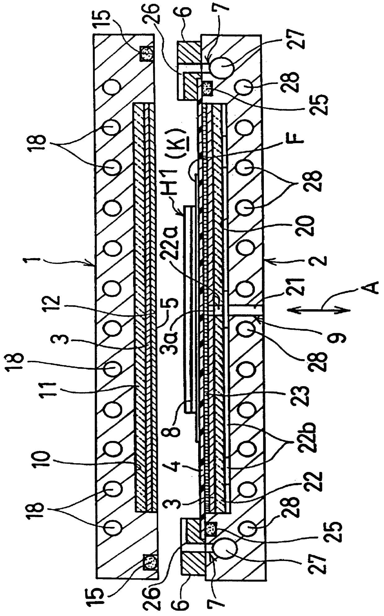
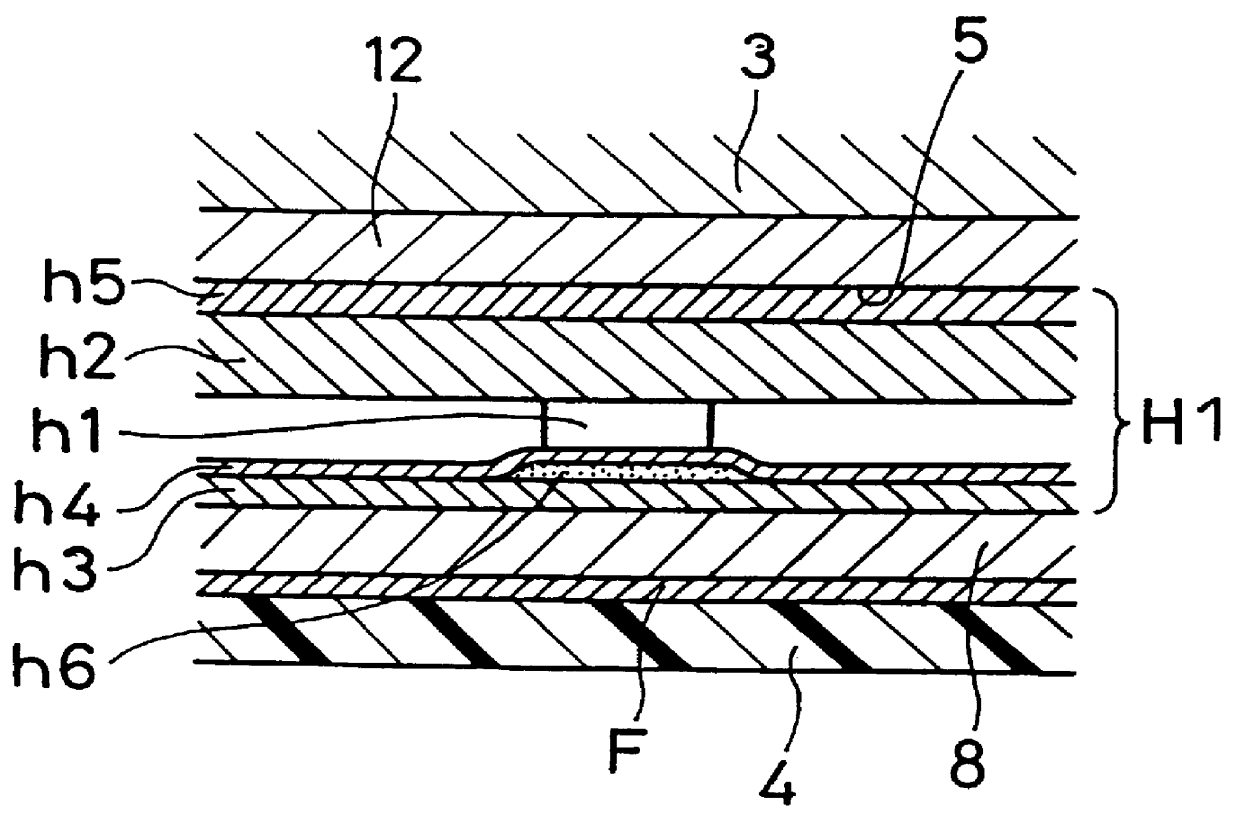
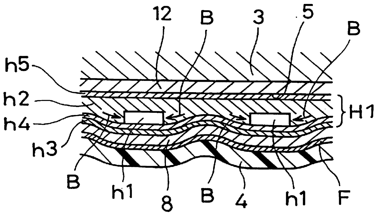
The lamination molding method and embodiments of the lamination molding apparatus will be explained in detail based on the attached drawings. In figures, identical signs indicate the identical or corresponding portion. First, the lamination molding method and apparatus is explained based on FIGS. 1-5. For reference, in this embodiment, the lamination member of the material H1 is an IC chip or the coil (hereinafter referred to as "IC chip etc.") h1 and the product molded in being embedded with the IC chip etc. h1 is an IC card, the laminate-molding apparatus is explained in accordance with the case where one of the pair of smooth pressurizing plates is formed with a resiliently deformable pressurizing plate 8 is pressurized by a film body 4 provided on either one of the opposing surfaces of the upper platen 1 and the lower platen 2.
The lamination molding apparatus of the present invention, as shown in FIG. 1, in general, while the material H1 comprises the IC chip etc. h1 and the res...
second embodiment
Next, the lamination molding method of the present invention is in detail explained according to the case where, using the lamination molding apparatus constituted as mentioned above and mainly based on FIG. 7-9, the circuit substrate is laminate-molded. The lamination molding method of the pesent invention comprises the steps of, in general, overlapping the circuit substrate ha and the resin layer hb having the insulation property, disposing these between the smooth surface 5 having rigidity and the film body 4 having the flexibility provided so as to be able to pressurize these to the smooth surface 5 in such a manner as the resin layer hb having the insulation property contacts to the smooth surface 5 when it is pressurized by the film body 4 and the circuit pattern ha 2 of the circuit substrate ha contacts to the film body 4, depressurizing between the circuit substrate ha and the resin layer hb having the insulation property and therearound without pressurizing these, melting t...
third embodiment
Next, the lamination molding method and apparatus of the present invention is explained in accordance with the case where the circuit substrate is used for laminate-molding the circuit substrate based on FIGS. 6, 10-13. For reference, in this embodiment, the same and corresponding signs to the same and corresponding parts are used with same signs and explanations thereof are omitted.
The lamination molding apparatus of this embodiment of the present invention, in general, in which the material H2' comprises the circuit substrate ha formed with the circuit pattern ha 2 on the surface of the insulating layer ha 1 and the resin layers hb, hb having at least the insulation property which are laminated on both sides of the circuit substrate ha, is for making the surfaces of the resin layers hb, hb having the insulation property smooth, and that apparatus comprises the upper
platen 1 and the lower platen 2 which are provided in opposing manner to come close to and separate from each other, ...
PUM
| Property | Measurement | Unit |
|---|---|---|
| Pressure | aaaaa | aaaaa |
| Flexibility | aaaaa | aaaaa |
| Moldable | aaaaa | aaaaa |
Abstract
Description
Claims
Application Information