

Modification of interfacial fields between dielectrics and semiconductors
a technology of dielectrics and semiconductors, applied in the direction of semiconductor devices, semiconductor/solid-state device details, electrical apparatus, etc., can solve the problems of low current gain of transistors, and achieve good control of deposition rate and stoichiometry
- Summary
- Abstract
- Description
- Claims
- Application Information
AI Technical Summary
Benefits of technology
Problems solved by technology
Method used
Image

Examples
example i
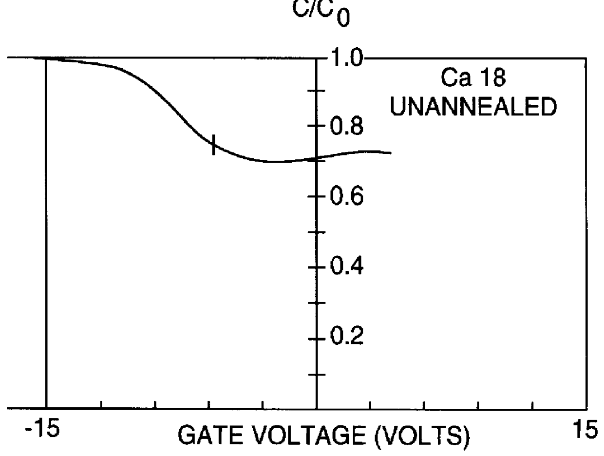
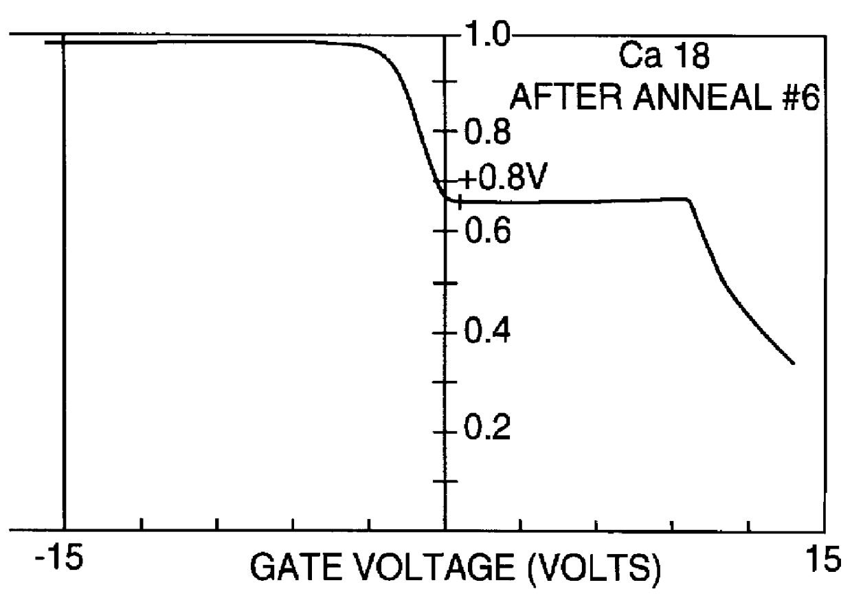
Layers of oxide were thermally grown on wafers of 6-9 ohm-cm n-type 100 silicon. The average thickness of the oxide layers was 770 angstroms.+-.10 angstroms.
The wafers were divided into three groups. One group of wafers was implanted with calcium at a dose of 1.times.10.sup.12 cm.sup.-2. A second group of wafers was implanted with calcium at a dose of 1.times.10.sup.13 cm.sup.-2. A third group, which functioned as the control group, was implanted with krypton at a dosage of 1.times.10.sup.13 cm.sup.-2. The implant energies were chosen so that the predicted range (R.sub.p) for each implant would be in the oxide near the SiO.sub.2 / Si interface.
All of the samples were then annealed in the following sequence:
1. 450.degree. C. for 40 minutes in a forming gas comprised of 80% N.sub.2 and 20% H.sub.2.
2. 1100.degree. C. for 30 minutes in pure nitrogen.
3. 450.degree. C. for 40 minutes in the forming gas.
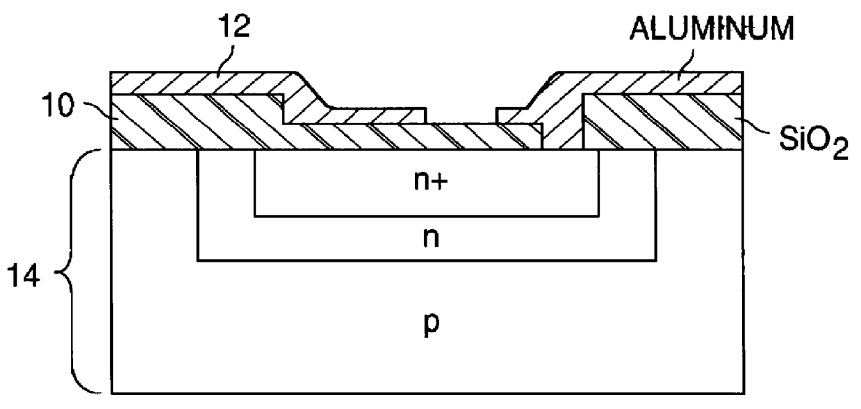
MOS capacitors each having a silicon dioxide dielectric 10 interposed between an aluminu...
example ii
Layers of oxide were grown on silicon wafers. The wafers were SEH, 100, p-type, 11-18 ohm-cm substrates and SEH, 100, n-type, 5-9 ohm-cm substrates. The oxide layers were grown with dry HCl process at 900.degree. C. to a thickness of 750 angstroms.
The samples were implanted with calcium at respective doses of 10.sup.12, 10.sup.13 and 10.sup.14 cm.sup.2. The implant energy was chosen at 70 KeV so that R.sub.p was about 560 angstroms. This depth insured that the distribution peak of the calcium remained on the oxide side of the silicon dioxide / silicon interface after annealing.
MOS capacitors were formed, and the samples were annealed in the following sequence:
1. 450.degree. C. for 20 minutes in a mixture of 90% N.sub.2 and 10% H.sub.2.
2. 750.degree. C. for 30 minutes in pure nitrogen.
3. 450.degree. C. for 20 minutes in a mixture of 90% N.sub.2 and 10% H.sub.2.
4. 905.degree. C. for 30 minutes in pure nitrogen.
5. 450.degree. C. for 20 minutes in a mixture of 90% N.sub.2 and 10% H.sub.2....
example iii
Samples having oxide layers with a thickness of 750 angstroms were implanted with calcium at a dosage level of 10.sup.14 cm.sup.-2 and an implant energy of 70 KeV, as in Example II. The distribution of the calcium was determined using secondary ion mass spectroscopy (SIMS). The results of this determination are shown in FIG. 4a.
The samples were then annealed in the following sequence:
1. 500.degree. C. in 90% N.sub.2, 10% H.sub.2 for 40 minutes;
2. 950.degree. C. in 100% N.sub.2 for 30 minutes;
3. 500.degree. C. in 90% N.sub.2, 10% H2 for 40 minutes.
The distribution of the calcium was again determined, and the SIMS data is shown in FIG. 4b.
A comparison of the data shown in FIGS. 4a and 4b reveals that the distribution of the calcium is substantially unaffected by the annealing process. Thus, the energy level for the implant process can be chosen so that Rp falls within the final range of desired locations for the additive species.
Since atoms of the alkaline earth metals strontium and b...
PUM
| Property | Measurement | Unit |
|---|---|---|
| temperature | aaaaa | aaaaa |
| thickness | aaaaa | aaaaa |
| biased temperature | aaaaa | aaaaa |
Abstract
Description
Claims
Application Information