Plasma reaction apparatus and plasma reaction

Inactive Publication Date: 2000-10-10
SEMICON ENERGY LAB CO LTD
View PDF14 Cites 34 Cited by
  • Summary
  • Abstract
  • Description
  • Claims
  • Application Information

AI Technical Summary

Benefits of technology

The present invention provides a plasma reaction apparatus, e.g. a film deposition apparatus, of a parallel planar type comprising electrodes being arranged in parallel with each other at a distance of 10 mm or less. The rate of film deposition can be increased by thus setting the electrodes. Furthermore, a film having an improved step coverage can be realized by irradiating an ultraviolet light to the electrode during the film deposition. In addition to the aforementioned constitution of the apparatus, two pairs of parallel planar type e

Problems solved by technology

However, none of the enumerated processes satisfy both of the deman

Method used


Image

  • Plasma reaction apparatus and plasma reaction
  • Plasma reaction apparatus and plasma reaction
  • Plasma reaction apparatus and plasma reaction

Examples


example 2

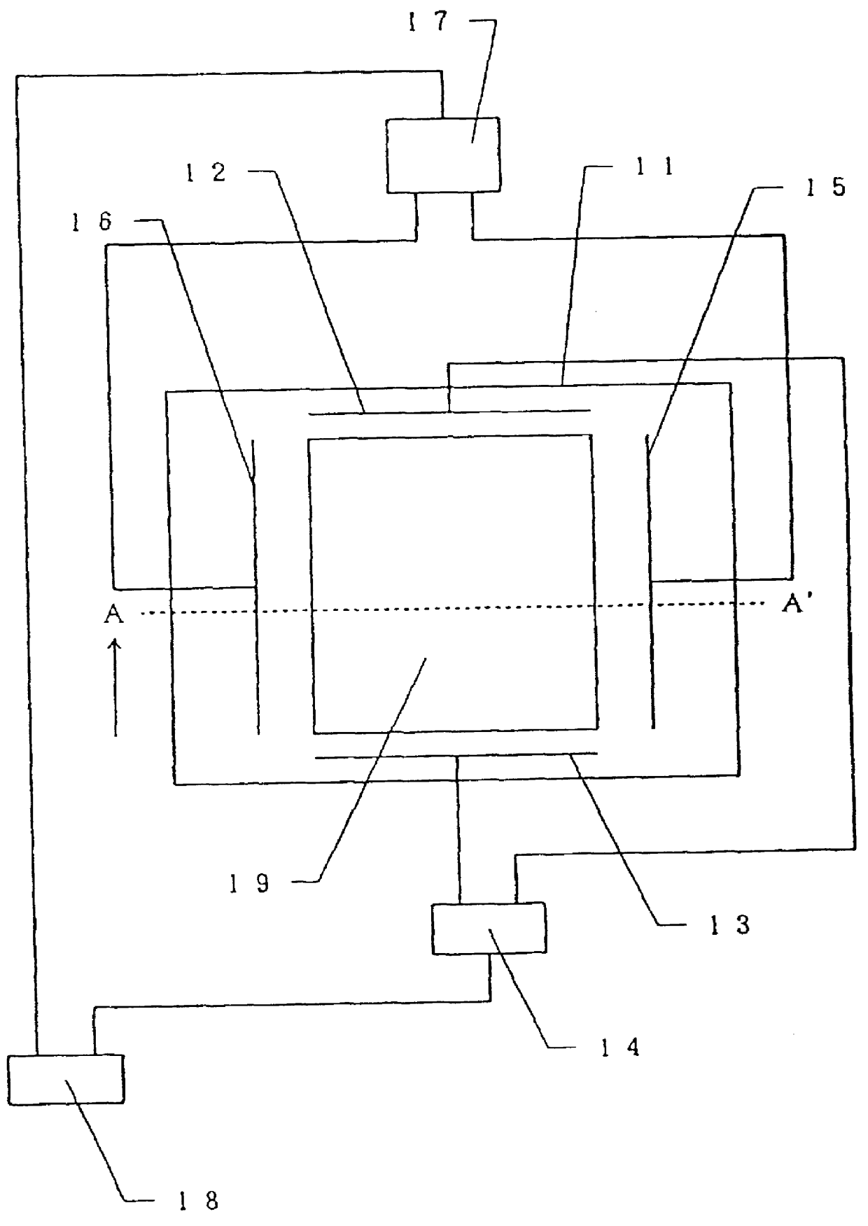
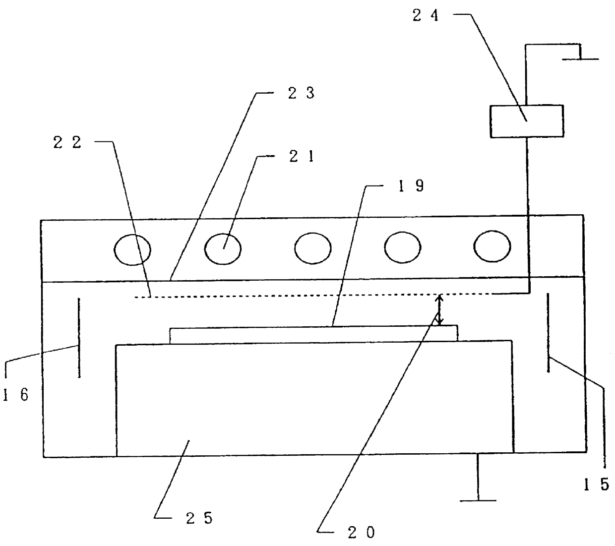
The present example relates to a process for depositing a silicon oxide (SiO.sub.2) film by using a film deposition apparatus illustrated in FIGS. 1 and 2. Tetraethoxysilane (TEOS; Si(OC.sub.2 H.sub.5).sub.4) was used as the starting gas for the film deposition in this example, but other organic silanes having ethoxy groups can be used as well, for example, Si(OC.sub.2 H.sub.5).sub.4, Si.sub.2 O(OC.sub.2 H.sub.5).sub.6, Si.sub.3 O.sub.2 (OC.sub.2 H.sub.5).sub.8, Si.sub.4 O.sub.3 (OC.sub.2 H.sub.5).sub.10, and Si.sub.5 O.sub.4 (OC.sub.2 H.sub.5).sub.12.

The film deposition is effected by applying high frequency power (50 MHz) to each of the two pairs of electrodes, i.e., to the pair of the electrodes 12 and 13, as well as to the pair of electrodes 15 and 16 which are crossed with the electrodes 12 and 13 in such a manner that one pair make a right angle with respect to the other pair. The high frequency power applied to one pair of the electrodes has a constant phase difference, gener...

example 3

The present embodiment comprises, in addition to the film deposition process of Example 2 comprising irradiating ultraviolet light during the film deposition, annealing the thus deposited film while irradiating ultraviolet light to the deposited film. In this manner, for example, the interface properties of the gate insulation film of a TFT can be considerably improved. Furthermore, the effect of annealing can be further enhanced by heating the film in the temperature range of from about 200 to 500.degree. C., preferably, at about 350.degree. C., while irradiating the ultraviolet light.

example 4

The present embodiment comprises depositing a Si film using the film deposition apparatus described in Example 1. The film can be deposited by using silane (SiH.sub.4) or any of the reaction gases generally used in the deposition of a non-single crystal silicon film and hydrogen gas, optionally together with a doping gas, such as phosphine (PH.sub.3) and diborane (B.sub.2 H.sub.6).


PUM

PropertyMeasurementUnit
Distanceaaaaaaaaaa
Frequencyaaaaaaaaaa
Frequencyaaaaaaaaaa

Abstract

A process for depositing a film at a high rate and with superior step coverage properties, which comprises installing a pair of electrodes crossing with another pair of electrodes making a right angle with respect to the another pair, and applying a high frequency power differing in phase to the electrodes in order to apply a high frequency power having a Lissajous' waveform in the reaction space during the deposition of a film on a substrate.

Description

1. Field of the InventionThe present invention relates to a plasma reaction apparatus, particularly an apparatus for depositing a film such as a semiconductor film and an insulation film. The present invention also relates to a plasma reaction method, particularly a process for depositing a film.2. Prior ArtConventionally known processes for depositing semiconductor films and insulation films include plasma CVD, sputtering, low pressure CVD, and photochemical vapor deposition. However, none of the enumerated processes satisfy both of the demands of high speed deposition and high step coverage at the same time.Accordingly, an object of the present invention is to provide a process for depositing a film, which enables the deposition of a film at a high speed and yet, with an excellent step coverage. Another object of the present invention is to provide an apparatus for depositing a film which realizes the film deposition process above.SUMMARY OF THE PRESENT INVENTIONThe present invent...

Claims


Application Information

Patent Timeline
IPC IPC(8): C23C16/509C23C16/517C23C16/50H01L21/02H01J37/32H01L21/316C23C16/48H01L21/205H01L21/31
CPCC23C16/509H01L21/316H01J37/32082C23C16/517H01L21/02211H01L21/0217H01L21/02164H01L21/02274
Inventor YAMAZAKI, SHUNPEI
Owner SEMICON ENERGY LAB CO LTD
Why Eureka
Try Eureka