Vertical MOSFET and method of manufacturing thereof

a technology of vertical mosfet and manufacturing method, which is applied in the direction of semiconductor devices, basic electric elements, electrical apparatus, etc., can solve the problems of vertical mosfet, and achieve the effect of preventing the deterioration of the insulation breakdown voltage and low parasitic capacitan

Inactive Publication Date: 2000-10-17
RENESAS ELECTRONICS CORP
View PDF7 Cites 41 Cited by
  • Summary
  • Abstract
  • Description
  • Claims
  • Application Information

AI Technical Summary

Benefits of technology

An object of the present invention is to provide a vertical MOSFET and a method of manufacturing the vertical MOSFET, which i

Problems solved by technology

However, in the above-mentioned conventional vertical MOSFET has a problem
Further, there is a problem with the gate oxide film 1

Method used


Image

  • Vertical MOSFET and method of manufacturing thereof
  • Vertical MOSFET and method of manufacturing thereof
  • Vertical MOSFET and method of manufacturing thereof

Examples


first embodiment

A method of manufacturing the n-channel vertical MOSFET according to the present invention will now be described with reference to FIGS. 3A to 3F.

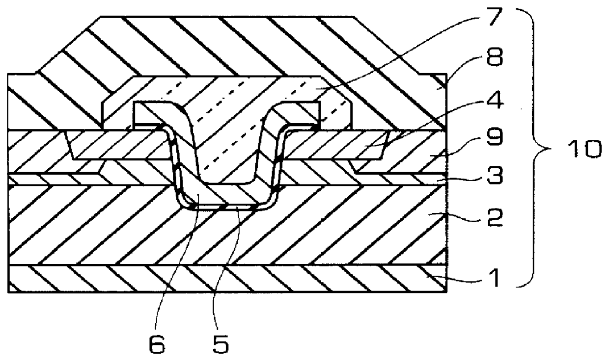
A wafer 10 has an n.sup.- -type epitaxial layer 2 of about 5 .mu.m in thickness doped with a phosphorus (P) of about 2.times.10.sup.16 cm.sup.-3 formed on the n.sup.+ -type semiconductor substrate 1. The semiconductor substrate 1 has a crystal face that is (100), whose orientation flat face is (100) and which has been doped with arsenic (As) of about 2.times.10.sup.19 cm.sup.-3.

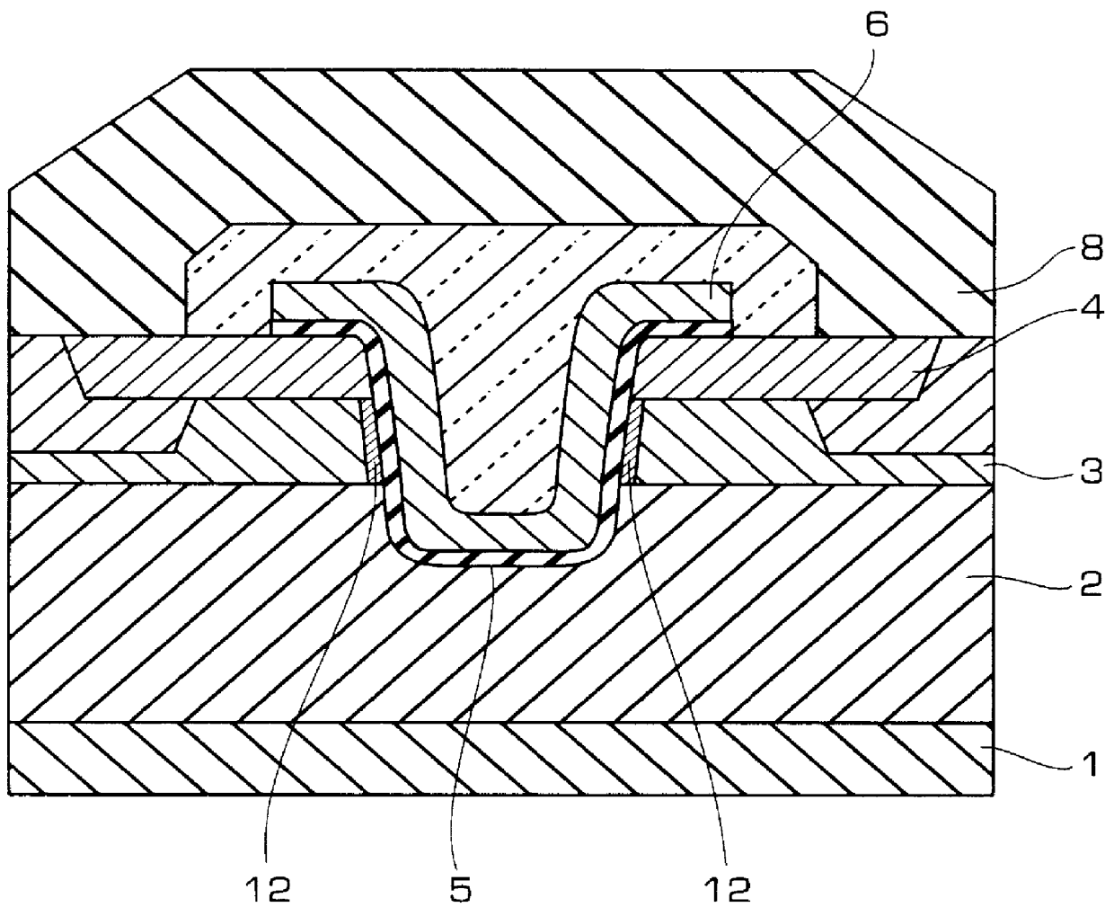
In FIG. 3A, first, an oxide film 15 of about 500 angstrom is formed on the n.sup.- -type epitaxial layer 2 of wafer 10. A nitride film 16 of about 1500 angstrom is then formed on the oxide film 15. Subsequently, the oxide film 15 and the nitride film 16 are patterned through the lithography technology, respectively. Parts of the oxide film 15 and the nitride film 16 (portions that form a groove) are sequentially removed through reactive ion etching (RIE).

Then, a res...

second embodiment

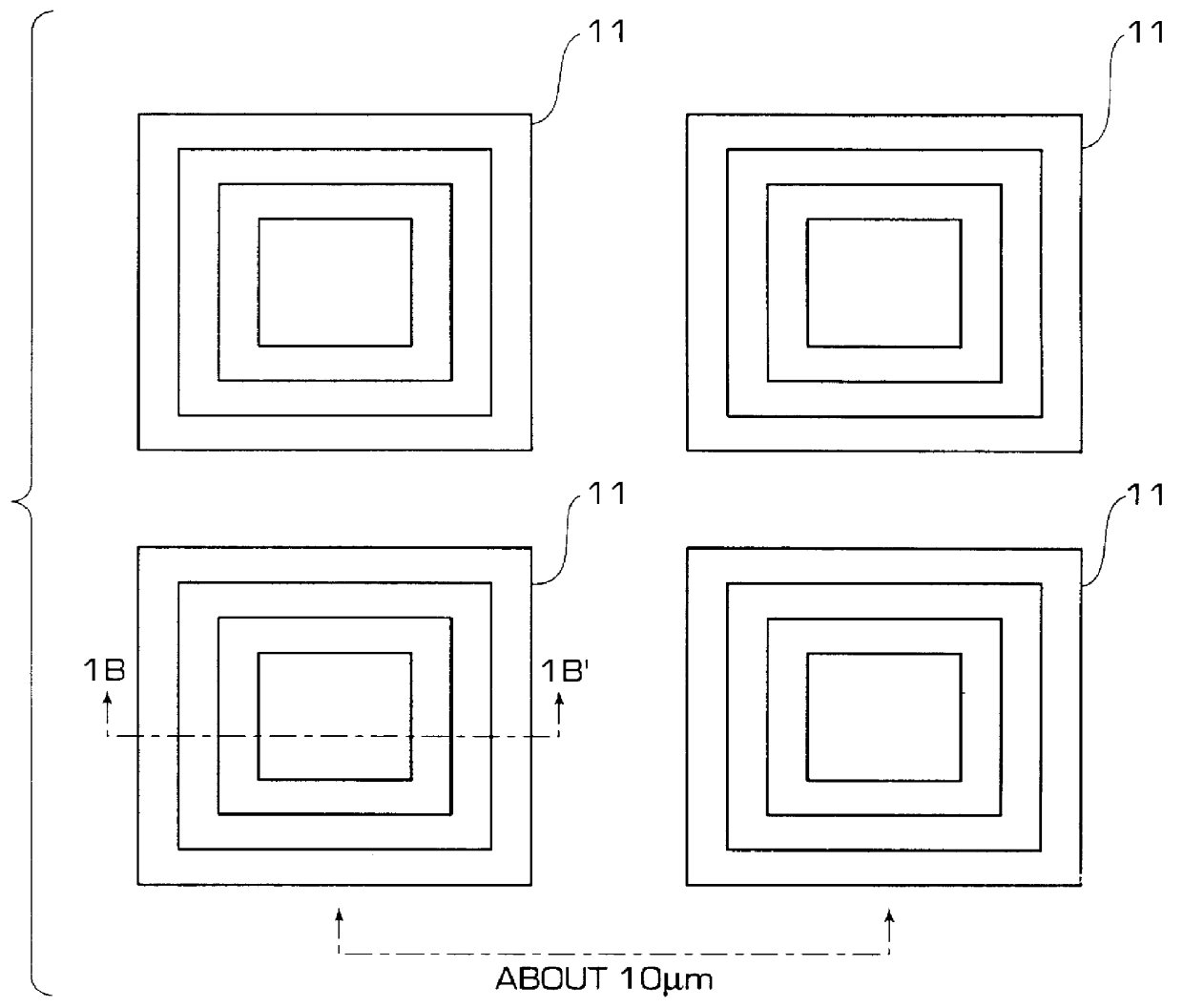
A method of manufacturing a vertical MOSFET according to the present invention will now be described with reference to FIGS. 6A to D, using an example of a p-channel type vertical MOSFET. The wafer used is a p.sup.- -type epitaxial layer 22 being formed on a p.sup.+ -type semiconductor substrate 21. A plurality of unit cells (the dimension of the unit cell is about 10 .mu.m) are formed on a main surface of the wafer in the shape of a lattice.

In FIG. 6A, first, phosphorus ions are implanted in a portion of the main surface of the wafer which forms a unit cell, and then thermally diffused until its depth becomes about 1.2 .mu.m, to thereby form an n-type base region 23. Subsequently, with a resist film formed as a mask through lithography, an n.sup.+ -type base contact region 29 and a p.sup.+ -type source region 24 are formed, respectively.

Then, as shown in FIG. 6B, an oxide film 35 and a nitride film 36 are sequentially formed on the n.sup.+ -type base contact region 29 and the p.sup...


PUM


Abstract

A vertical MOSFET of the present invention comprises a semiconductor wafer having a groove selectively etching in the semiconductor wafer to have substantially vertical side walls. The groove is oxidized using local oxidation of silicon (LOCOS) at 1100.degree. C. or greater to form a LOCOS film on the semiconductor wafer in the groove so that a whole side surface of said semiconductor wafer exposed by the groove is substantially vertical and essentially flat. The LOCOS film in the groove is removed and a thermal insulating film on the semiconductor wafer in the groove. Then a gate electrode made of a conductive film is formed on the thermal insulating film. An interlayer insulating film is formed on the gate electrode and a source electrode is formed in ohmic contact with a source region and a base region. A drain electrode is connected to the opposite side of the semiconductor wafer. As a result, the vertical MOSFET of the present invention has improved on-state resistance, reduced parasitic capacitance and higher breakdown voltage.

Description

BACKGROUND OF THE INVENTIONThe present invention relates to a semiconductor device and the method of manufacturing the semiconductor device, and more particularly to a vertical field effect transistor and the method of manufacturing the vertical field effect transistor.A vertical field effect transistor (hereinafter referred in to "vertical MOSFET") has been used over a variety of industrial fields in recent years because the vertical field effect transistor is simple in its drive circuit and can operate in a high-frequency region since it has excellent frequency characteristic, etc. The vertical field effect transistor is used over various fields, and thus demands increased performance has occurred. For example, demand for reduction of a resistant value (on-state resistance) during operation and reduction of a parasitic capacitance, as well as other characteristic has increased recently.As a means for reducing the resistant value during operation, there has been proposed a structur...

Claims


Application Information

Patent Timeline
IPC IPC(8): H01L21/02H01L21/336H01L21/316H01L29/78
CPCH01L29/78H01L21/316H01L29/42368H01L21/76235H01L29/7813H01L21/02107
Inventor SAWADA, MASAMI
Owner RENESAS ELECTRONICS CORP
Why Eureka
Try Eureka