
Device, in particular a semiconductor device, for processing two waves, in particular light waves

a semiconductor and light wave technology, applied in the field of light waves, to achieve the effect of low polarization sensitivity, simple, cheap and compact, and facilitate the development of optical fiber interactive networks

Inactive Publication Date: 2000-11-14
OCLARO NORTH AMERICA
View PDF8 Cites 21 Cited by
  • Summary
  • Abstract
  • Description
  • Claims
  • Application Information

AI Technical Summary

Benefits of technology

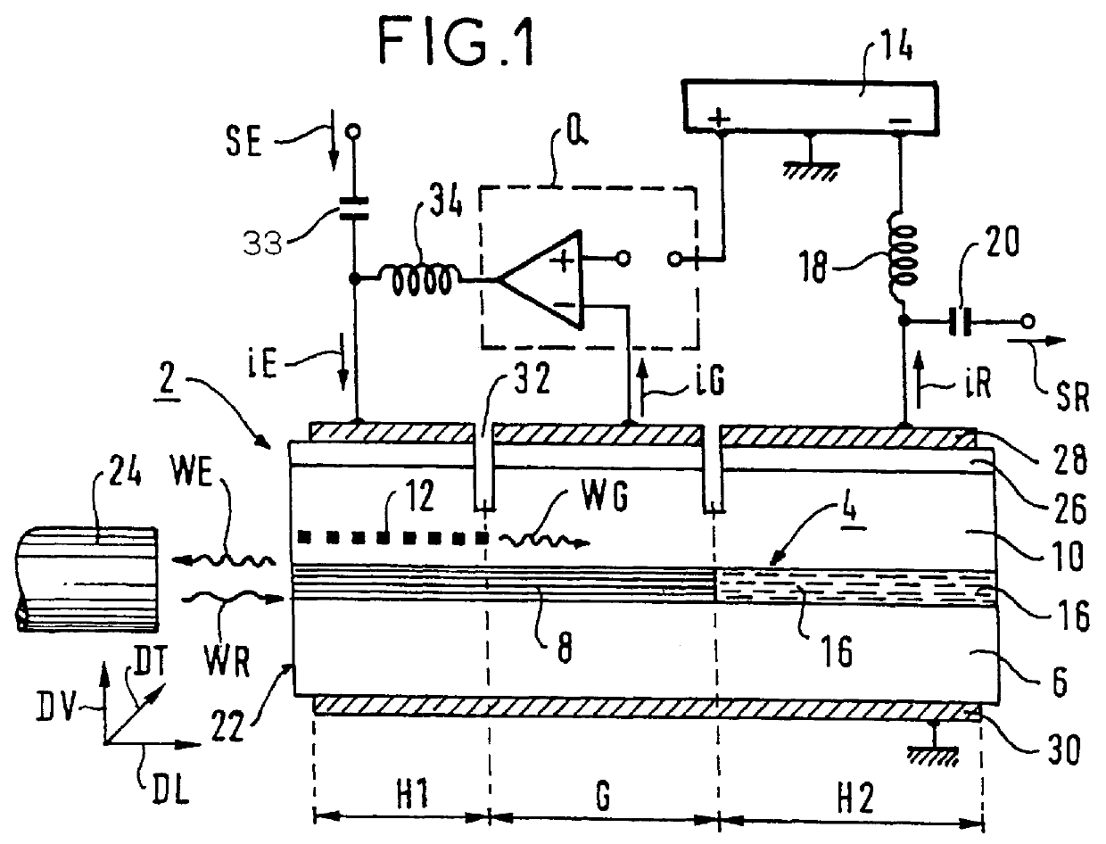
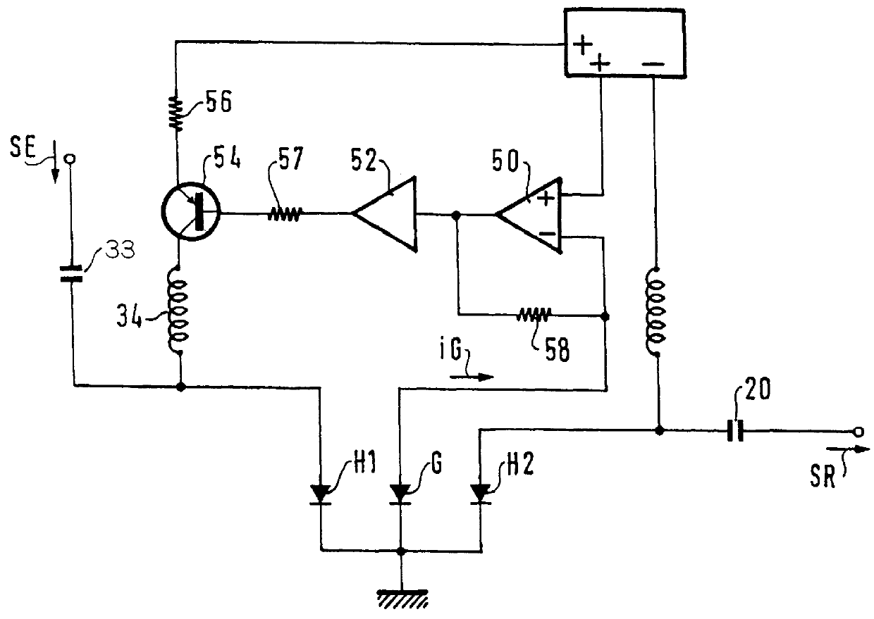
An object of the present invention is also to solve the second problem in a manner that is simple, cheap, and compact. For this purpose, the device of the invention further includes absorption measurement means delivering an absorption measurement signal representative of the power of the waves absorbed by said separator so as to constitute information on operation of said first processing member. Advantageously, said absorption measurement means may regulate operation of the first processing member, in particular when the processing performed by said operation is emission of waves having the first wavelength.
Although the invention is described above in general manner, it is more particularly and advantageously applicable when the waves in question are of the optical type, and travel along optical fibers. It is known that the considerable development of "multimedia" services is facilitating the development of optical fiber interactive networks, in particular local area networks. That type of network requires end devices to be used and installed on subscriber premises, and such devices must be high-performance, robust, and very cheap to enable the services in question to be mass-distributed. More precisely, as regards their performance, such devices must be capable of receiving optical signals at data rates of up to 622 Mbit / s with very low sensitivity to polarization, and they must be capable of emitting signals at data-rates of more than 155 Mbit / s. An advantageous configuration in the networks in question consists in using simultaneous both-way transmission. The end devices must then be of the transceiver type, i.e. each such device must perform the functions of emission at a first wavelength, and of reception at a second wavelength. It must also include an additional member enabling the up channels and the down channels (and thus the wavelengths) to be separated, thereby making it possible for information to be interchanged in both directions and simultaneously.
Furthermore, the device must be capable of operating under difficult conditions, i.e. over a temperature range from -40.degree. C. to +85.degree. C. (without using a Peltier-effect regulator). To ensure that the emitter member included in the device operates well, regulation must then be performed by servo-controlling the current powering the member on the optical power emitted by it. The power must therefore firstly be measured. The present invention provides a simple way of measuring the power.

Problems solved by technology

When, in addition, the two members are to be situated close together in a medium enabling the two waves in question to propagate, implementing suitable protection for the member to be protected then constitutes a first problem.

Method used


Image

  • Device, in particular a semiconductor device, for processing two waves, in particular light waves
  • Device, in particular a semiconductor device, for processing two waves, in particular light waves
  • Device, in particular a semiconductor device, for processing two waves, in particular light waves

Examples


first embodiment

The first embodiment given by way of example comprises a semiconductor chip 2 made up of layers succeeding one another in crystal continuity from bottom to top in a vertical direction DV defined relative to said chip. The chip includes a waveguide 4 extending in a horizontal longitudinal direction DL also defined relative to said chip, for guiding two light waves respectively having said first wavelength and said second wavelength. The second wavelength is longer than the first wavelength. Both the chip and the waveguide successively include the following going forward along the longitudinal direction DL:

a first processing segment H1 belonging to said first processing member;

a separation segment G belonging to said separator; and

a second processing segment H2 belonging to said second processing member.

To avoid cluttering the figures, said segments are designated by the same references as the members of which they constitute the respective parts included in the chip 2.

The separation ...

second embodiment

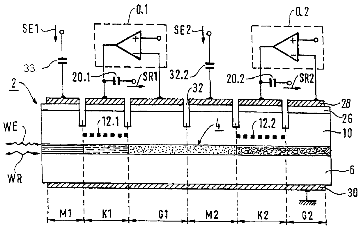
the invention (see FIG. 2) is generally analogous to the first embodiment, but it differs therefrom in the manner indicated below.

It includes a succession of six segments M1, K1, G1, M2, K2, and G2. The segments K1 and K2 are respectively analogous to the segments H1 and H2 of the first device except for two differences: firstly, each of them can perform emission and / or reception functions. Secondly, in performing their emission function, they do not act as modulators, modulation being performed by the respective modulation segments M1 and M2. The segment G1 both protects the segments M2, K2, and G2 against waves having the first wavelength, and also regulates the laser emitter constituted by the segment K1 provided with a Bragg grating 12.1. The only function of the segment G2 is to regulate the laser constituted by the segment K2 by means of a Bragg grating 12.2.

The modulation segments M1 and M2 are biased by means (not shown) under a reverse voltage of about -3 V. The characteris...


PUM

PropertyMeasurementUnit
wavelengthsaaaaaaaaaa
temperatureaaaaaaaaaa

Abstract

A common InP semiconductor substrate device includes a laser emitter H1 for emitting waves having a first wavelength such as 1,300 nm, a photodiode H2 for receiving and detecting waves having a second wavelength such as 1,550 nm, and a separator G absorbing the waves having the first wavelength, the separator being interposed between the laser emitter H1 and the photodiode G for protecting the photodiode against the waves having the first wavelength. An absorption measurement mechanism Q delivers a signal iG representative of the power of the waves absorbed by the separator G, to make it possible to regulate operation of the laser emitter H1. The semiconductor substrate device is particularly applicable to implementing end devices to be installed on subscriber premises for subscribers to optical fiber interactive local area networks.

Description

The present invention generally relates to processing to be performed on two waves having different wavelengths. The processing considered is, for example, emitting or modulating such a wave, or receiving such a wave for the purpose of retrieving a signal that was carried by said wave. The waves to be processed may, in particular, be of the radio, acoustic, or optical types.The invention is applicable when the two waves in question are to be processed respectively in two distinct members, and when one of the members is to be protected against the waves of the other member in that, if the member to be protected receives the waves processed or to be processed by the other member, operation of the member to be protected is disturbed. When, in addition, the two members are to be situated close together in a medium enabling the two waves in question to propagate, implementing suitable protection for the member to be protected then constitutes a first problem.OBJECTS AND SUMMARY OF THE IN...

Claims


Application Information

Patent Timeline
Patent Type & Authority Patents(United States)
IPC IPC(8): G02B6/12G02B6/42H01S5/026H01S5/00H01S5/0683G02F1/025
CPCG02B6/12004G02B6/4246H01S5/0262H01S5/0683H01S5/0264
Inventor JACQUET, JOELGURIB, SALIMDOUKHAN, FRANCISLE QUELLEC, HUGUES
Owner OCLARO NORTH AMERICA
Learn More